
Application Notes : kSA MOS – Curvature Based Real-Time Stress
Version: 1.0
- Introduction
- Techniques for Real-Time Stress Management
- Curvature Formalism
- Methods for Curvature Measurement
- MOS Apparatus
- Practical Considerations
- Select Examples of Data Acquisition and Interpretation
- Heteroepitaxy of Alloys on Si
- Plastic deformation
- Coherent Island Formation
- Ge Surface Segregation
- Deposition of Polycrystalline Metal Thin Films
- Practical Aspects
- Scientific Interpretation
- Conclusion
- References
- Figures
Curvature-based Techniques for Real-Time Stress Measurement During Thin Film Growth
Jerrold A. Floro and Eric Chason
Sandia National Laboratories, Albuquerque, NM 87185-1415
The severe kinetic constraints often imposed during thin film deposition can produce highly non-equilibrium microstructures that support stress levels far above the corresponding bulk yield stress. Such high stress levels have important, and often deleterious, consequences for the film performance and reliability. At its most extreme, stress can cause film failure through delamination of the film from the substrate, film cracking, surface roughening, or mass transport. Failure can occur during or immediately after disposition, during subsequent film processing, or during field service. At a lesser extreme, stress and strain can modify the relevant properties of a film, including the tribological, mechanical, magnetic, electrical, and optical properties. This is usually an unwanted effect, but in some cases, for example, in devices incorporating epitaxial semiconductor strained layers, strain is used to tailor electronic or optoelectronic properties. Finally, strain fields interact with chemical and transport processes in thin films, affecting the energetics and kinetics of interdiffusion and phase transformations.
Despite intensive research efforts exploring the origins of stress in thin films, much is still poorly understood about how stress develops during film growth, or how stress relaxes. Stress evolution is intimately tied to the microstructural and surface evolution of a film, which in turn depends strongly on the deposition process and conditions. It is common to classify stress as extrinsic or intrinsic. Extrinsic stress might arise from a deliberately-applied external stress during growth, but the most common source of extrinsic stress in thin films results from thermal mismatch, i.e., the difference between the film and substrate thermal expansion coefficients, coupled with a variation in temperature during or after deposition. More scientifically interesting is the so-called intrinsic stress (better term: the growth stress) that arises when a structurally evolving thin film is constrained against changes in its in-plane dimension because it is rigidly bonded to a substrate. “Structurally evolving” encompasses a variety of processes, including island coalescence, grain growth, heteroepitaxy, impurity incorporation, point defect formation or annihilation, phase transitions accompanied by volume changes, surface structural and morphological evolution, momentum transfer effects from energetic particle bombardment, etc. In certain situations the picture is dramatically simplified – this is true in the case of “simple” epitaxial systems such as Si1-xGex/Si, which we will discuss in some detail later because it elegantly demonstrates the usefulness of real-time, curvature-based stress diagnostics. However, we note that the vast majority of film/substrate/process combinations result in polycrystalline films with complex microstructures, and correspondingly complex stress evolution.
It is not the purpose of this article to review in detail the origins of growth stresses in thin films. The reader is referred to excellent reviews in the literature [Nix 1987; Doerner and Nix 1988; Koch 1994]. Rather, our intent is to demonstrate the advantages gained in understanding the origins and relaxation of thin film stress by measuring stress evolution in real-time during thin film growth. The evolution of stress and strain in thin films during deposition and annealing is typically studied by sequentially iterating the process parameters and applying ex situ analysis, the so-called “cook-and-look” approach. This approach is straightforward but labor-intensive. Experiments in which the dynamic stress/strain evolution is measured in real-time during growth are becoming more common. Real-time measurements are more efficient, and they can provide unique information on strain evolution that would be unobtainable through cook-and-look.
It is also worth noting that curvature-based stress measurement can potentially be used for real-time process control monitoring of thin film growth and processing. Whereas research applications for real-time stress monitoring typically place a premium on sensitivity and acquisition frequency, for process-control applications the emphasis is on long-term measurement stability, robustness, and simplicity or operation.
We will focus here on the use of curvature-based stress measurement techniques, which offer the greatest degree of versatility and compatibility with the film deposition environment. In particular, we describe in detail a curvature technique called the multi-beam optical sensor (MOS) that has characteristics that make it quite useful in both the research and process-control environments. After a discussion of the formalism and techniques for curvature analysis, we will review results obtained during growth of epitaxial SiGe on Si, and during deposition of polycrystalline metal films. Again, the intent is not to exhaustively review the science, but to illustrate the use and interpretation of real-time curvature data.
Techniques for Real-Time Stress Management
We begin with a brief survey of approaches to stress or strain measurement that have been used previously as in situ or real-time diagnostics.
Certainly the most accurate means to determine the complete strain state of a thin film is x-ray diffraction (XRD) [Clemens 1992]. XRD is not generally useful for real-time measurement of strain in the laboratory due to the long acquisition times required and the expense and complexity of the tooling. Time-resolved strain measurements during growth are typically only possible with very bright sources such as the synchrotron. In situ synchrotron studies of the lattice parameters of very thin metal films have been carried out during sequential growth interruptions, making the technique quasi-real-time [Lairson et al. 1995].
Reflection high energy electron diffraction (RHEED), which is standard instrumentation on most molecular beam epitaxy (MBE) chambers, has been applied to real-time measurement during film growth. RHEED allows straightforward measurement of the lattice constant at the surface of a growing epitaxial film [Price 1988; Whaley and Cohen 1990], although its use for strain determination in a polycrystal in not precluded a priori. RHEED typically requires a vacuum environment, and therefore cannot be used during sputtering or chemical vapor deposition (CVD) without additional effort to reduce electron scattering in the source and beam-path. RHEED can also suffer from a sensitivity to stray magnetic and electrostatic fields associated with electron-beam evaporation sources and substrate heaters, which can greatly increase measurement noise and background drift unless special precautions are taken.
The vibrating membrane technique can measure thin film stress in real-time with excellent sensitivity (on the order of 0.02 MPa) [Su and Wuttig, 1993; Berry and Pritchett 1990; Berry et al. 1990]. Knowledge of film thickness is not required in order to determine the stress. Furthermore, measurement of the film’s internal friction can be obtained concurrently with the stress measurement. Restrictions associated with the practical use of this technique include the need for the specialized membrane substrate, the ability to measure only tensile stress, and the requirement of a high vacuum ambient in order to avoid atmospheric damping. Quartz resonators have also been used to measure stress, thickness, and temperature during growth, but, obviously, this approach has a built-in substrate restriction that limits general application [Way 1993].
Raman spectroscopy is a powerful tool for spatially- and temporally-resolved stress measurement that has been applied during annealing and external stress loading in dielectric thin films [Exharos and Hess 1996]. Raman has not, to our knowledge, been used during thin film growth, and the technique is only applicable to a relatively narrow set of materials. Similar remarks apply to photoluminescence spectroscopy [Ma and Clarke 1993].
The most commonly used technique for real-time stress measurement is the substrate curvature, or bending beam, approach. Here the stress is determined by measuring the change in substrate curvature induced by the film stress. In practice there are many experimental approaches to measure the substrate curvature. Taken together, curvature-based approaches offer the best overall compromise between versatility, simplicity, sensitivity, and compatibility with a variety of film deposition processes. The rest of this article is devoted to a review of curvature-based approaches.
Curvature Formalism
Consider a cubic, isotropic thin film under stress. The lateral dimension of the film/substrate couple are taken to be much larger than the thickness of the couple. In the absence of external loading, the stress state of a continuous, planar thin film is equibiaxial, i.e.,  . The in-plane strain in the film is then simply determined from
  .
.  is the biaxial modulus,
  , where
  is Young’s modulus and v is Poisson’s ratio. Cubic, anisotropic films that are in the {111} or {001} orientation (texture or epitaxy) will still be isotropic in-plane, so that
  . must now be calculated appropriately in terms of the material stiffness, Cij as follows [Nix, 1989]:
![\[ \{001\} \quad M = c_{11} + c_{11} - \frac{2c^2_{12}}{c_{11}} \quad \quad (1a) \]](https://k-space.com/wp-content/ql-cache/quicklatex.com-84144cec6550773582124e36843b28e1_l3.png "Rendered by QuickLaTeX.com")
![\[ \{111\} \quad M = \frac{6c_{44} (c_{11} + 2c_{12})}{ c_{11} + 2c_{12} + 4c_{44}} \quad \quad (1b) \]](https://k-space.com/wp-content/ql-cache/quicklatex.com-945a9437f296e51372edfff147ec38f3_l3.png "Rendered by QuickLaTeX.com")
For cubic, anisotropic films in lower symmetry orientations (e.g., {110}), the stress will in general only be biaxial, where now  , but all other stress components are still zero. The relation
  is still valid, but the value of
  will depend on in-plane direction.
It is worth noting that near the edges of the film, the stress state is more complicated, with nonzero shear components. However, the shear stress magnitude drops off rapidly with distance from the edge, and is typically negligible for distances greater than 5hf, where hf is the film thickness [Doerner and Nix 1988]. Thus for blanket films, essentially all of the film is in a pure biaxial stress state, but for patterned films, e.g., interconnect lines with high aspect ratio, or in the case where films consist of three-dimensional islands, shear stresses will be significant.
A biaxially-stressed film exerts forces on its substrate, creating both biaxial stress in the substrate, as well as exerting a bending moment that curves the substrate (Figure n-1). For a film that is much thinner than the substrate, the film is essentially unmodified by the compliance and bending of the substrate. The curvature,  , of the substrate is then very simply related to the mean biaxial film stress,
  as:
as:
![\[ \kappa = \frac{1}{R} = \frac{6 \sigma_f h_f}{M_s h_s^2} , \quad \quad (2) \]](https://k-space.com/wp-content/ql-cache/quicklatex.com-58888f91a87ad453fe639f0ed896dcc1_l3.png "Rendered by QuickLaTeX.com")
where  is the radius of curvature,
  is the substrate biaxial modulus, and
  is the substrate thickness.
Equation (2), often called Stoney’s equation [Stoney 1909], is the central relation connecting substrate curvature to film stress. It can be derived either through mechanical equilibrium approaches, where the internal forces and bending moments are summed to zero [Hoffman 1976], or by an equivalent elastic energy minimization approach [Flinn 1987]. More complete theories that relax the thin film approximation, and are applicable to multilayer or graded layer structures, have also been derived [Freund 1996; Townsend et al. 1987].
We next summarize a number of important aspects of Stoney’s equation relevant to stress measurement in thin films.
- Equation 2 is strictly true only when the substrate is flat prior to film deposition, which is often not the case. It is the change in curvature that is required in order to obtain the film stress accurately. Therefore, for post-deposition determination of film stress, the absolute curvature both before and after deposition must be measured. However, in real-time measurement, the change in curvature is obtained by definition, and the absolute initial curvature is not needed.
- The curvature is inversely proportional to the square of the substrate thickness. Therefore, for maximum sensitivity, as is required in surface science experiments, very thin wafers should be used. However, for depositions producing thicker films with large stresses, thicker wafers should be used to avoid finite deflection effects, as discussed below.
- Curvature-based approaches to stress measurement require independent knowledge of film thickness. During deposition, both thickness and stress will be evolving, in general. Thus accurate knowledge of the deposition rate is required in order to quantify the real-time stress evolution.
- The film stress-thickness product is often called the “force/width” and is given in units of N/m or dyn/cm. Alternatively it can simply be referred to as the “stress-thickness”, given in units of GPa-Å or equivalent. For post-deposition measurement,
 should be replaced with the integrated stress,
  , which explicitly acknowledges that the stress can have a through-the-thickness variation that cannot be determined solely by post-deposition curvature measurement. For real-time measurement during deposition, the evolution of curvature will be expressed by
![\[ \left(\frac{M_s h_s^2}{6}\right) \frac{d \kappa}{dt} = \sigma_f^{(gs)} \dot{h}_f + \int^{h_f}_{0} \frac{d \sigma_f }{dt} dz + \frac{d(\Delta F)}{dt} \quad \quad (3) \]](https://k-space.com/wp-content/ql-cache/quicklatex.com-a21a3e14bb042b96a6b1b47ec7191467_l3.png "Rendered by QuickLaTeX.com")
The meanings of the terms on the right-hand side of Eq. 3 are illustrated in Figure n-2. The first term, where  is the bulk lattice stress at the growth surface and
  is the deposition rate, represents the contribution to the evolving curvature from material arriving from the vapor. The second term represents any depth-dependent relaxation processes occurring in the already deposited film. The third term generically accounts for the contribution from the surface stress
  [Cammarata 1994; Doerner and Nix 1988] due to evolution in surface crystallography, morphology, or chemistry. Note that if the relaxation rate is independent of depth, then the first and second terms become simply
  . Then Eq. 3 integrates to Stoney’s equation, with the surface stress included explicitly.
Others in the literature refer to the incremental stress, obtained by taking the first derivative of the stress-thickness vs. thickness data obtained in real-time [Shull and Spaepen 1996]. The incremental stress so obtained in proportional to dk/dt in Eq. 3. We note that in order to differentiate typical curvature data, smoothing or filtering must be applied to remove high frequency noise.
In addition to the incremental stress, one can also define the mean stress, which is obtained simply by dividing the stress-thickness by the film thickness. The mean stress is thus simply equal to S/hf.
- In the thin film approximation (i.e.,
 ), different layers will contribute independently and additively to the curvature [Townsend et al 1987; Nix 1989]. In other words, the stress in one film does not substantially modify or create stresses in underlying layers (including substrate).
 - When does the thin film approximation used to derive Eq. 2 become inaccurate? As the film becomes an appreciable fraction of the substrate thickness, the induced biaxial compression or extension of the substrate in response to the forces imposed by the film can relieve a measurable portion of the film stress. Freund has shown that for a uniformly equi-biaxial stressed film having mismatch strain
 , the curvature is given to second order in hf/hs by [Freund 1996; Freund 1997]
![\[ \frac{\kappa}{\kappa_S} = 1 + \frac{h_f}{h_s} \left( 1-4 \frac{M_f}{M_s} \right) \quad \quad (4) \]](https://k-space.com/wp-content/ql-cache/quicklatex.com-03cdbb9316a5c805dff78f05a18f8141_l3.png "Rendered by QuickLaTeX.com")
where  is the first order curvature from Stoney’s equation (Eq. 2). Therefore the relative error associated with using Stoney’s equation will be
  . The error is plotted in Figure n-3 as a function of hf/hs, parameterized by the ratio of substrate and film moduli. For
  and typical modulus ratios, Stoney’s equation is accurate to within 5%.
- Even in the regime where the thin film approximation is accurate, Stoney’s equation can fail if the substrate curvature becomes large enough such that the out-of-plane deflections associated with bending produce non-vanishing shear strain components [Freund 1997]. In this case the external dimension of the substrate will now become important. For the case where the film and substrate have equal biaxial moduli, the relation between the substrate curvature, film strain, and film thickness is the finite deflection regime is given by [Freund 1997]
![\[ \frac{6B^2 h_f h_s \varepsilon^{(m)}}{h^4} = \frac{K}{16} \left[ 16 + K^2(1-v) \right] \quad \quad (5) \]](https://k-space.com/wp-content/ql-cache/quicklatex.com-e28268a5ade2e8ff0fed8929cb881732_l3.png "Rendered by QuickLaTeX.com")
where B is the diameter of the circular substrate,  is the extensional mismatch strain between the film and substrate,
  . This equation is exact for all values of film and substrate thickness. For
  , and for
  , Eq. 5 reduces to Stoney’s equation. In Figure n-4 we plot the curvature vs. film thickness from Eq. 5 (we have taken so that
  , for simplicity). We also plot the Stoney curvature for comparison. For a film with 1% strain (common in heteroepitaxy) on a 2 inch diameter substrate that is 300 um thick, the effect of finite deflections is negligible up to 8000 Å (see Figure n-4A). However, for the same film on a wafer only 100 µm thick (common in research applications requiring high sensitivity), the effect can be quite significant, as shown in Figure n-4B.
Eventually, if the substrate curvature becomes too large, it will cease to bend symmetrically on a spherical surface, i.e.,  . For a uniform film with equibiaxial stress on a circular substrate of radius B, the critical strain at which bifurcation in the deformation occurs is given by [Freund 1997]
![\[ \varepsilon^{(m)} = \frac{4}{3(1+v)^{3/2}} \frac{h^2_s}{B^2} \frac{h_s}{h_f} \left(1 + \frac{h_s}{h_f} \right)^4 \quad \quad (6) \]](https://k-space.com/wp-content/ql-cache/quicklatex.com-31c201fcdb2724708801ab3c3ba88b86_l3.png "Rendered by QuickLaTeX.com")
For example, using a 2 inch diameter wafer that is 100 µm thick, depositing a film with 1% strain, the deformation mode will become asymmetric at about 1600 Å. This regime can be experimentally accessible during low temperature epitaxy.
Methods for Curvature Measurement
There are many approaches to measuring the curvature of a substrate. They can be roughly classed as point deflection, laser deflectometry, height analysis, and lattice-bending. Deflectometry will be the focus of this article, but we first briefly discuss other techniques.
Point Deflection: The deflection of a single point of a sample, usually shaped as a rectangular strip, and mounted in a springboard configuration (Figure n-5), can be measured, and related to the curvature as
![\[ \kappa = 1/R = \frac{2}{(B^2 - d^2)^{1/2}} \sin \left[ \tan^{-1} \left( \frac{d}{B} \right) \right] \quad \quad (7) \]](https://k-space.com/wp-content/ql-cache/quicklatex.com-4d0ad66fd3ccb3276e1142017eafa9c7_l3.png "Rendered by QuickLaTeX.com")
Where is the radius of curvature,  is the length of the substrate from the mounting point to the measurement point, and d is the deflection. The deflection can be measured directly in real-time using a microscope and video camera [Gill and Clyne 1994]. However, while it is simple to carry out, this approach suffers from a lack of sensitivity (0.1 GPa-Å [Sander and Ibach 1991], but the apparatus is relatively complex and specialized, and therefore is not easily integrated into the typical deposition environment.
Height Analysis: The height of a curved wafer, z(x,y), can be measured directly, either using a stylus profilometer, or via optical interferometry. Profilometry is relatively simple, but lacks sensitivity, and it is not a viable real-time technique. Optical interferometry could, in principle, be performed in real-time, although we are unaware of this being done. Sensitivity is likely to be poorer than that obtained with laser deflectometry approaches.
Lattice-bending: If the substrate is a single crystal, then it is possible to detect and directly measure the bending of the lattice planes parallel to the surface by a sequential set of measurements across the sample surface [Segmuller et al. 1980]. At each measurement point, the sample is rotated to maximize the intensity of the Bragg reflection. The sample is then translated linearly to the next measurement point, and the process is repeated. The change in rotation required to keep the maximum x-ray intensity, as a function of lateral position, is then used to determine the curvature.
Laser Deflectometry: Consider a laser beam incident normal to a flat, reflective sample at point A, as shown in Figure n-6A. The position of the reflected spot on a screen or position sensitive detector a distance L from the sample is also shown. Now translate the beam to point B, a distance D0 away (while retaining the normal incidence). The reflected spot will, of course, move an identical distance. Now cause the sample to bend, as shown in Figure n-6B, and repeat the measurement. Upon translating the beam the same linear distance D0, the reflected spot moves a distance D that is different from D0 due to the sample curvature. The curvature I given by  , where
  . This is true so long as both
  and
and  . Actual laboratory implementation of laser deflectometry, then, whether for real-time applications or for benchtop use, is a matter of illuminating multiple points across the sample surface, and detecting the change in the reflected spot position. Three different approaches to accomplishing this procedure have been developed.
Translational scanning: In this approach, either the laser/detector assembly, or the sample, is physically translated laterally with respect to the other, performing exactly the measurement just described [Pan and Blech 1984]. This is conceptually simple, and commercial stress measurement apparatus based on this approach are available. However, translational scanning is not optimal for real-time measurement during deposition, where motion of the sample is typically undesirable, and motion of the laser is cumbersome and slow.
Rotational scanning: Using a fixed laser and sample position, the beam may be scanned across the sample by first reflecting it from a rotating mirror, as shown in Figure n-7. This scans angle as well as position (i.e., the angle of incidence is varying). However, if a long focal length lens is inserted between the mirror and substrate, with the mirror is precisely on the focal plane of the lens [Flinn 1987], the rotational scan is converted to a pure translational scan. The reflected beams pass back through the same lens and are incident upon a position sensitive detector (PSD), which also lies on the focal plane. This approach has the convenient attribute that if the sample is flat, the reflected beam position will be independent of the incident beam position on the sample. For a curved sample, the reflected beam will translate along the PSD as the beam is scanned along the sample. Rotational scanning has been implemented quite successfully for real-time measurements during annealing [Flinn 1987; Volkert 1991b], ion implantation [Volkert, 1991a], and deposition [Shull and Spaepen 1996]. It is very sensitive, able to measure radii of a curvature up to 40 km on the benchtop [Flinn 1987]. However, in a vibrationally noisy ambient, such as is typical for film deposition chambers, the actual sensitivity is typically limited to be on the order of 1 km [Volkert 1991a; Shull and Spaepen 1996]. Scanning techniques (both rotational and translational), are inherently sensitive to vibration because the measurements are made serially. This problem is overcome by the multi-point illumination approach.
Multi-point illumination: Instead of scanning a single beam serially, the multi-point approach simultaneously illuminated the sample with multiple laser beams. A variety of experiments have been carried out using a single laser and a beam-splitter to provide two-beam illumination [Kobeda and Irene 1986; Martinez and Golovchenko 1990; Schell-Sorokin and Tromp 1990; Leusink et al. 1992]. Detection is accomplished with a quadrant photodiode. As the substrate bends during deposition, the distance between the beams changes in proportion to the curvature. In situ sensitivities of up to 10 km have been reported [Martinez and Golovchenko, 1990]. The authors have extended the two-beam approach to a true multi-beam approach that we call the Multi-beam Optical Sensor (MOS) [Floro et al. 1996b; Floro et al. 1997a; Taylor et al. 1997]. This technique is described in detail in the following section.
The Multi-Beam Optical Sensor (MOS)
MOS improves upon the two-beam approach in a number of ways. The essential apparatus is schematically illustrated in Figure n-8A. MOS uses a single lower power laser. The beam is divided into a linear array of multiple parallel output beams by transmission through an etalon, which is a piece of optical glass with parallel faces, and each face has a high-reflectivity optical coating. The reflectivity  is in the range 93-98%. The linear beam array then reflects off the sample and is detected on a camera. The only other optics are a spatial filter, an objective lens to focus the beam on the camera, and attenuating filters, if necessary, to prevent saturation of the camera.
The video camera, with a standard 480×640 pixel format, is connected to a personal computer through a frame grabber. Commercial controller and acquisition software determines and records the centroid position of each spot on the camera as a function of time. The separation D(t) (see Figure n-8B) between each adjacent beam is related to the local change in curvature ](https://k-space.com/wp-content/ql-cache/quicklatex.com-7684e824ee73786d5e906a482da45b62_l3.png "Rendered by QuickLaTeX.com") , where L is the distance from the sample to the camera array, and
, where L is the distance from the sample to the camera array, and  is the angle of incidence.
MOS offers a number of advantages for use as a real-time stress monitor for thin film deposition. Relative to the rotational scanning approach, MOS has the advantage of using simultaneous multipoint illumination and detection. This reduces the sensitivity to ambient vibration since the laser beams move in a coupled fashion, whereas in a serial scan, vibration creates uncorrelated noise between each measurement. Routine measurements of substrate radii as large as 4 km on a vibrationally noisy deposition chambers have been performed, with no special provisions for vibration isolation [Floro et al. 1996b]. Radii of curvature of up to 20 km have been measured on the benchtop, limited primarily by the pixel size of the camera. Sensitivity could be improved by use of a higher density camera array. Another limitation with a standard camera is the overall dimension (about 0.6×1 cm). This constrains the substrate area that can be measures to be no larger than the video array.
MOS requires no moving parts and optical alignment is straightforward, making the apparatus robust and very simple to use. Ease of operation is further enhanced by use of video imaging of the output beam array. camera-based detection is much simpler when more than two beams are used, and imaging of the beam array allows for easy alignment and focusing prior to deposition. The use of multiple beams permits either local curvature measurement (with a minimum lateral resolution of about 1.5 mm), or noise reduction through appropriate averaging over the beam array. Temporal resolution is also good – with a fast computer measurements can be at nearly the video rate of 30 Hz.
Practical Considerations
We next cover some practical considerations in the use of MOS for real-time measurement during deposition. Two basic requirements are obvious – the use of an optically reflective substrate, and optical access to the substrate during growth.
Substrate Mounting: The substrate must be mounted so that it is free to bend along at least one axis during deposition. One possibility is a springboard configuration, where the sample is in the shape of a rectangle strip and is clamped at one end (see Figure n-5). If the length of the strip is much larger than the width, then biaxial bending can be assumed and Eq. (2) maybe used. Springboard mounting tends to exhibit higher vibrational noise, however, than in free-mounting.
Free-mounting allows for unconstrained bending of the substrate. This is trivial in deposition systems where the sample simply rests face-up on a platen. In situations where this is not possible, an alternative free-mounting scheme uses a perimeter cage, as shows in Figure n-9. If sample heating is required, heat coupling must be radiative, as conductive coupling is very poor in this configuration. Wafer temperature can only be measured optically – thermocouple attachment cannot be easily made without affecting the bending. Using spring-clips to hold the sample, and the use of attached thermocouples, may be permissible if the wafer is large enough so that the contacted regions are far away from the region being measured.
Other more specialized schemes can be envisaged. One worth mentioning here is the E-shaped substrate [Shull and Spaepen 1996]. The outer legs are clamped and may have thermocouples attached, while the middle leg is free to bend.
Sample Rotation: Some deposition processes require rotation of the sample about its normal center axis to provide uniform thickness or stoichiometry of the MOS beams across the camera array with each revolution. This problem can be minimized by synchronously triggering camera acquisition with each rotation of the substrate.
Number of Useful Beams: The spacing between the beams is controlled by the angle of incidence of the input beam on the etalon. Accurate measurement of beam spacing requires that the beam intensity profiles do not overlap. Therefore the maximum number of beams that can be used in MOS is given by the ratio of the camera dimension to the full width of the laser spots. While physical reduction of the spot size through focusing optics is limited, the spots size may be effectively reduced by adjusting the background level of the video camera, without deleterious effect on the measurement accuracy. The number of useable spots will also be limited by the decreasing intensity of each successive beam imposed by the etalon. For an etalon with coatings of reflectivity SYMBOL on each face, the intensity spot is  . Higher reflectivity provides more uniform intensities, but reduces the absolute intensity incident upon the sample. If absolute intensity is too low, a simple “fix” is to remove the reflective coating at the point where the input beam impinges, which increases the output intensity by a factor of
  .
.
Two-dimensional Beam Arrays: If a second etalon is inserted into the beam path, and oriented orthogonal to the first, a 2D grid of laser beams is produced. This permits simultaneous measurement of both principal curvatures [Chason and Floro 1996]. Output intensity is severely reduced with two etalons, but the fix mentioned above helps alleviate this.
Reflectivity Changes: Significant changes in sample reflectivity can occur during deposition, for example, when a metal film is deposited on an optically transparent substrate. These changes will exceed dynamic response of the camera. This can be accounted for by manually inserting attenuation filters as required. A more elegant solution is to use a diode laser and feedback on the reflected intensity signal from the camera to control the laser output power.
Changes in surface roughness will change the intensity of the specularly-reflected laser beams due to an increasing diffusely-scattered component. This can be used as a qualitative measure of roughness evolutions.
For thick dielectric films, interference between light reflected from the top and bottom surfaces of the film can be used to measure the thickness and deposition rate simultaneously with the stress, assuming the index of refraction is known [Brieland and Killeen 1995].
Thermally-Induced Curvature: Thermal curvature signals present a challenging problem when making sensitive real-time measurements of the growth stress during deposition. By “thermal curvature” we mean changes in the real or apparent substrate curvature associated with temperature fluctuations during deposition, or due to thermal gradients within the sample.
Temperature fluctuations: When film deposition is initiated, for instance by evaporation or sputtering, the temperature of the substrate will increase. The temperature rise can be anywhere in the range of a few degrees to several hundred degrees. If the film and substrate have different coefficients of thermal expansion, significant curvature evolution will occur due solely to the thermal mismatch stress. This can completely mask the evolution of the growth stress. Shull and Spaepen have examined this problem in detail and show that temperature measurement during deposition, as well as independent knowledge of the effective thermal mismatch and substrate modulus, can accurately correct for thermal curvature evolution [Shull 1996; Shull and Spaepen 1996].
Thermal gradients: Thermal gradients in the wafer along the axis normal to the substrate plane will induce curvatures in the substrate. For instance, consider the case wherein a clean wafer is receiving a constant heating power from the back, and all heat losses out the front side are purely radiative. Lateral conductive losses are ignored. Then, in steady-state, a linear temperature profile will be established, and the difference between the back and front side temperatures will be  , where
  is the emissivity,
  is the Stefan-Boltzmann constant,
  is the temperature of the front side, is the substrate thickness, and
  is the thermal conductivity. The induced curvature from the linear temperature gradient will be given by
  , where is the coefficient of thermal expansion. Note that the curvature is independent of substrate thickness. Finally, the apparent stress-thickness due to the temperature gradient is given by
![\[ (\sigma h)^{\mathit{apparent}} = \frac{M_s h_s^2 \alpha e \sigma_{sb} T_f^4}{3K} \quad \quad \quad (8) \]](https://k-space.com/wp-content/ql-cache/quicklatex.com-923117310d8cb72ea6daa5efb8424a4a_l3.png "Rendered by QuickLaTeX.com")
This is plotted in Figure n-10 for several thicknesses of a Si wafer. Thermal gradient effects will be most noticeable at high temperature, and for thicker substrates that have poor thermal conductivity. Thermal gradients in the plane of the substrate can also produce changes in curvature, depending on the geometric distribution of the gradients and the external constraints on the sample
Double-Sided Growth: In some film growth processes, such as oxidation, films are grown simultaneously on both sides of the substrate. Even if the films are in a state of stress, the curvature will not evolve due to the compensating effects of the front and back side.
Select Examples of Data Acquisition and Interpretation
Here we provide examples on the use and interpretation of real-time stress measurement using laser deflectometry during this film deposition. This is a narrow but illustrative selection of experimental results that demonstrate the power of the technique. We present results obtained during the deposition of heteroepitaxial semiconductors and polycrystalline metal thin films. In this section it should become apparent to the reader that real-time measurement provides a significant advantage in efficiency and scientific value-added over iterative post-deposition measurement. Nonetheless, the evolution of curvature during growth can be complex and subject to correspondingly complex interpretation. Therefore, the real-time data must always be supported with ex situ analysis of the film’s microstructural or chemical evolution.
Heteroepitaxy of Si1-xGex Alloys on Si (001)
 alloys grown epitaxially on Si are of technological interest due to their potential for use in heterostructure-based, high performance microelectronics that can be integrated into standard Si process technology [Bean 1992’ Wang and Karunasiri 1993]. The lattice mismatch strain in the alloy is
  .
.  provides a model system for the study of epitaxial growth and strain relaxation, and in the best understood heteroepitaxial system. In this section briefly summarize results of real-time stress measurements, made using MOS, during plastic deformation, coherent island formation, and surface segregation.
Plastic deformation
Strained  films can relax their lattice-mismatch strain through the nucleation and glide of misfit dislocations. Below a certain thickness,
  , dislocation propagation in thermodynamically forbidden [Matthews et al. 1970; Freund 1990]. Above this thickness, dislocations form subject to kinetic constraints. The critical thickness and the relaxation kinetics can be efficiently mapped out using MOS. In Figure n-11 we show the stress-thickness as a function of film thickness during deposition by molecular beam epitaxy (MBE) of
  at three different temperatures. For growth of a coherent (i.e., fully elastically strained), planar alloy at constant deposition rate, we expect that the curvature, or stress-thickness, will increase linearly with time, since the stress is constant, and the thickness increases linearly with time (see Eq. 3). This linear regime is observed for all three temperatures in Figure n-11 [Floro et al. 1997a]. However, for all three films the curvature evolution becomes sub-linear as misfit dislocations relax the stress. At higher depositions temperatures, relaxation occurs earlier and proceeds more rapidly. This we directly measure the kinetic critical thickness in a single run. The equilibrium critical thickness can also be measured, in principle, if we grow at sufficiently high temperature, although competition from surface roughening may complicate the interpretation.
The time dependence of the mean strain,  , provides the relaxation kinetics during growth or annealing. Of course, the kinetics of dislocation nucleation, glide, and multiplication are convoluted in these curves. In order to separate the effects, other experiments and/or analyses are required [Volkert 1991b; Gillard and Nix 1993].
Coherent Island Formation
Strained epilayers can relax a portion of their strain through the formation of coherent islands. Coherent island formation provides a pathway to strain relaxation during lattice-mismatched heteroepitaxy that can bypass or at least precede the introduction of misfit dislocations [Mo et al. 1990; Eaglesham and Cerullo 1990; Guha et al. 1990]. Relaxation results from the evolution of the film geometry rather than through shear, and is kinetically mediated by surface diffusion. Geometric relaxation occurs because three dimensional islands are less constrained in-plane than the uniform film. The stress distribution within an island, and in the underlying substrate, is complex [Johnson and Freund 1997].
Real-time stress measurements during high temperature MBE growth of  have proven quite useful in the study of coherent islanding kinetics. Figure n-12 shows MOS curvature data obtained during deposition [Floro et al. 1997b]. Reductions in the slope of the stress-thickness vs. thickness data immediately indicate the onset of stress-relieving islanding transitions, which efficiently guides the application of ex situ analysis such as microscopy. Images of the corresponding surface morphologies, obtained by atomic force microscopy (AFM), are also shown in Figure n-12.
Or course, in a film comprised of 3D islands, the stress field will also be 3D, and highly non-uniform. Curvature-based measurements will yield an effective stress that corresponds to the mean biaxial stress in a film having the same mass-equivalent thickness.
For an analysis of the curvature evolution, the islanded film may be treated as a three-layer structure. The wetting layer, which is a planar film at the full coherency stress  , has (time-dependent) thickness
  . The island layer has a net mass-equivalent thickness of
  , where
  is the total thickness of material deposited at time
  . The effective stress of this layer can be expressed as
 ![g[A(t)] \sigma_{coh}](https://k-space.com/wp-content/ql-cache/quicklatex.com-62c6470463daec96975e10d86e2a58d1_l3.png "Rendered by QuickLaTeX.com") , where A is the aspect ratio (height-to-width) of the islands, and
, where A is the aspect ratio (height-to-width) of the islands, and  ranges from 0 to 1. can be determined by finite element analysis. Finally the third layer is the surface, which can have an evolving surface stress
  . The evolution of curvature during island formation can then be described by the following equation [Floro et al. 1997b]:
![\[ \frac{M_sh_s^2}{6} \kappa(t) = \sigma_{coh}h_{wl}(t) + g[A(t)]\sigma_{coh} \left[ h_f(t) - h_{wl}(t) \right] + \Delta F(t) \quad \quad (7) \]](https://k-space.com/wp-content/ql-cache/quicklatex.com-c3f666ff7e8b07dd5c06fe3121f2793e_l3.png "Rendered by QuickLaTeX.com")
Surface stress evolution is not significant in this case. In Figure n-12 the regime of deposition labeled as “huts” has a constant (albeit reduced) slope. From Eq. (7) this immediately implies that the island array is evolving with constant shape, which has been verified by ex situ analysis (surface stress and wetting layer thickness are assumed to be constant). The measured slope in the “hut” regime is  (i.e.,
 ![g[A] = 0.8](https://k-space.com/wp-content/ql-cache/quicklatex.com-4c8336748dcb12f44475c7f805cd4785_l3.png "Rendered by QuickLaTeX.com") ), in good agreement with predictions from finite element calculations.
), in good agreement with predictions from finite element calculations.
Ge Surface Segregation
During Si1-xGex/Si epitaxial growth, Ge segregates to the surface of the growing film in order to reduce the surface energy [Godbey and Ancona 1993]. Segregation has important and deleterious consequences for quantum wells devices, since it tends to leave a graded composition layer at the original growth interface, as shown in Figure n-13. This graded layer, which we call the denuded zone, is difficult to measure quantitatively ex situ, since its thickness is typically less than 20 Å. However, the Ge surface segregation process exhibits a time-dependent signature in real-time curvature data. This is shown in Figure n-14A, which plots the stress-thickness vs. thickness for low temperature growth of Si1-xGex/Si (001) films (x = 0.21, 0.3, 0.47). In the early stages of alloy growth, the films are planar and coherent, and thus a linear change in curvature with thickness is expected. Prior to this however, we initially observe a transient tensile stress. It is important to understand that this transient in the curvature arises only from changes in the surface stress associated with the development of the Ge-enriched surface during formation of the denuded zone. Even though the depth-varying Ge concentration in the denuded zone produces a depth-varying coherency stress, the curvature is not sensitive to this variation. In particular, the curvature does not depend on how the Ge is distributed through the depth of the film, but only on total amount of Ge deposited (as long as the film surface remains nearly planar and the Ge all resides on lattice-registered sites). This consequence of the fact that the lattice parameters of Si1-xGex/Si alloys obey Vegard’s Law, combined with the fact that curvature measures the stress integrated over film thickness. (Thus, curvature could not be used to measure interdiffusion of Si and Ge, but could be used to measure evaporative loss of Ge.) Further discussion of this somewhat subtle point may be found in [Floro et al. 1996a]. It is shown there that
![\[ \left( \frac{M_s h_s^2}{6} \right) \frac{d \kappa}{dt} = M \varepsilon_{Ge} R_{Ge} + \frac{d \Delta F}{dt} \quad \quad (8) \]](https://k-space.com/wp-content/ql-cache/quicklatex.com-38e4d81933a34a14d3930411993bd9ee_l3.png "Rendered by QuickLaTeX.com")
where  is the deposition rate of
  and
and  is the strain of pure Ge on Si (
 ). For constant , the observed non-linearities in
  can result only from changes in the surface stress . We can calibrate the evolution of with the thickness of the pure Ge segregation layer simply by growing pure Ge on Si while measuring curvature. This calibration then permits us to evaluate the time-dependent thickness of the segregation layer, which in turn can be used to reconstruct the composition profile of the denuded zone. The result is shown in Figure n-14B, derived from the data of the three films shown in Figure n-14A [Floro et at. 1996a]. The important point is that sensitive real-time curvature measurements using MOS permit efficient determination of the bulk composition profile resulting from surface segregation with monolayer thickness resolution, which cannot be done with any ex situ depth-profiling technique.
Deposition of Polycrystalline Metal Thin Films
Stress evolution in polycrystalline thin films can be considerably more complex than in epitaxial films. In this section we briefly review work by Shull and Spaepen (SS) for ultra-high vacuum (UHV) thermal evaporation of Ag and Cu onto thermally oxidized Si [Shull and Spaepen 1996; Shull 1996]. This work nicely brings out many aspects, both practical and scientific, of the use and interpretation of real-time curvature data.
Practical Aspects
SS measures film/substrate systems with much lower growth stresses, and much larger differential thermal expansions, than are present during Si1-xGex/Si epitaxy. As a result, it was necessary for SS to correct for thermal stresses arising from unwanted radiative heating or cooling of the sample when shutters controlling the deposition flux were opened and closed. Temperature variations of only five degrees produced curvature evolution during deposition of the same order as the growth stresses. SS measured the sample temperature concurrently with the curvature. This was done by using an E-shaped sample with thermocouples attached to the upper and lower arms of the E, while the middle arm was free to bend. Thermal loads were deliberately applies to films of known thickness to determine the product of the film biaxial modulus and the difference in thermal expansion coefficients between the film and substrate,  . Then, given the temperature history during deposition, the thermal contribution to the curvature could be removed from the raw data. Unfortunately, SS found literature values for , were not representative of thin films.
A typical result showing the thermal and intrinsic contributions to the measured curvature evolution is given in Figure n-15. Interestingly, the thermal effect is insignificant throughout most of the deposition, but strongly affects the data during post-deposition “annealing”.
SS also found that changes in room temperature affected the alignments of the scanning laser apparatus, causing baseline drift during long-term curvature acquisitions that are not accounted for by measurement of the sample temperature. The reduced criticality of alignments using the MOS technique instead of serial scanning may reduce the apparent drift, but this has not been verified.
Finally, for measurements of the evolution of stress in Ag and Cu, the UHV environment was found to be critical to obtaining good repeatability in the stress evolution. Abermann has shown previously that oxygen partial pressures of greater than 2×10⁻⁸ Torr can significantly affect the fil stress [Abermann and Koch 1986].
Scientific Interpretation
SS observed several prominent, repeatable features in their experiments on the stress evolution during deposition of Ag or Cu on SiO2, and deposition of Ag on Cu or Cu on Ag. All data discussed in this section has had thermal component of the curvature subtracted out as described above.
Figure n-15 shows the curvature during deposition of Ag on SiO2. Upon initiation of deposition, a small, transient compressive stress was observed. The origins of this transient are unclear, but may be related to changes in the net surface stress, and the formation of the Ag/SiO2 interfaces. Note that Ag grows in the Volmer-Weber mode on SiO2.
The stress subsequently becomes tensile and reaches a maximum value. Based on previous work by Abelmann, this tensile stress was associated with island coalescence and the formation of the continuous polycrystalline film with its network of grain boundaries [Abelmann and Koch 1985].
The stress then becomes compressive once again. The existence of this compressive regime had been controversial due to the thermal mismatch stresses present in all experiments. However, the careful determination of the thermal stress component by SS clearly indicates that an extended compressive regime of the growth stress does exist. The origins of this stress are not understood, but may be connected to the steady-state surface morphology established during growth.
If deposition is interrupted, the stress evolves towards tensile, as shown in Figure n-15. This is not simply relaxation of the compressive stress, since the evolution is independent of whether the stress at the end of deposition is net tensile or compressive. Interestingly, is deposition is resumed, the stress rapidly evolves back towards its original value when growth was first interrupted. This demonstrates that the tensile increase during the interrupt is not the result of a bulk process such as grain growth or vacancy annihilation, but must be associated with a reversible surface process.
Finally, by growing Ag on Cu or Cu on Ag, discontinuities in the curvature evolution were analyzed to show that the Ag/Cu interface stress in compressive. This agrees qualitatively with previous measurements, but disagrees with results of molecular static’s calculations using embedded atom potentials, which predict that the interface stress is tensile.
Conclusion
Curvature-based techniques offer the researcher a powerful ability to sensitively monitor stress evolution in real-time during this film deposition. A new approach, known as the Multi-beam Optical Sensor (MOS), is particularly suited for real-time applications due to its low sensitivity to vibration, and its simplicity of set-up and operation. MOS can be applied in the research environment, or as a process-control tool in development or production activities. Accurate evaluation of curvature data to obtain the true evolution of the growth stress may requite accounting for a number of effects, including the thermal history of the sample, and finite deflection effects, depending on the specific experimental situation. Real-time determination of film stress through curvature measurement can greatly enhance out understanding of the origins and evolution of growth stresses in thin films. Ex situ analysis of the film’s microstructural evolution is still required for definitive interpretation of curvature results, but the real-time data makes this process far more efficient than traditional cook-and-look approaches.
References
*Abermann, R. and Koch, R. (1985) Thin Solid Films 129, 71-.
*Abermann, R. and Koch, R. (1986) Thin Solid Films 142, 65-.
Bean, John (1992) Proc. IEEE 80 (4), 571-587.
Berry, B.S. and Pritchett, W.C. (1990) J. Appl. Phys. 67 (8), 3661-3668.
Berry, B.S., Pritchett, W.C., Cuomo, J.J., and Guarnieri, C.R. (1990) Appl. Phys. Lett. 57 (3) 302-303.
Breiland, W.G. and Killeen, K.P. (1995) J. Appl. Phys. 78, 6726.
Cammarata, R.C. (1994) Prog. Surf. Sci. 46(1), 1-38.
Chason, E. and Floro, J.A. (1996) Mater. Res. Soc. Symp. Proc. 428, 499-504.
Clemens, B. and Bain, J.A. (1992) MRS Bull. 17, 46-51.
Doerner, Mary F. and Nix, William D. (1988) Crit. Rev. Solid St. Mater. Sci. 14(11), 225-268.
Eaglesham, D.J. and Cerullo, M. (1990) Phys. Rev. Lett. 64 (16), 1943-1946.
Exharos, G.J. and Hess, N.J. (1996) J. Raman Spec. 27, 765-774.
Flinn, P.A., Gardner, D.S., and Nix, W.D. (1987) IEEE Trans. Elec. Dev. ED-34 (3), 689-699.
Floro, J.A., Chason, E., and Lee, S.R. (1996b) Mater. Res. Soc. Symp. Proc. 406, 491-496.
Floro, J.A., Chason, E., Lee, S.R., et al. (1997a) J. Elec. Mater. 26 (9), 969-979.
Floro, J.A., Chason, E., Twesten, R.D., Hwang, R.Q., and Freund, L.B. (1997b) Phys. Rev. Lett. 79 (20), 3946-3948.
Freund, L.B. (1990) J. Mech. Phys. Solids 38 (5), 657-679.
Freund, L.B. (1996) J. Mech. Phys. Solids 44 (5), 723-736.
Freund, L.B. (1997) in Mater. Res. Soc. Proc. 436, 393-404.
Gill, S.C. and Clyne, T.W. (1994) Thin Solid Films 250, 172-180.
Gillard, V.T. and Nix, W.D. (1993) Z. Metallkd. 84 (12), 874-880.
Godbey, D.J. and Ancona, M.G. (1993) J. Vac. Sci. Tech. B 11(3), 1120-1123.
Guha, S., Madhukar, A., and Rajkumar, K.C. (1990) Appl. Phys. Lett. 57 (20), 2110-2112.
*Hoffman, R.W. (1976) Thin Solid Films 34 185-190.
Kobeda, E. and Irene, E.A. (1986) J. Vac. Sci. Tech. B 4(3) 720-722.
*Koch, R. (1994) J. Phys: Condens. Matter 6, 9519-9550.
Lairson, B.M., Payne, A.P., Brennan, S. et al. (1995) J. Appl. Phys. 78 (7), 4449-4455.
Leusink, G.J., Oosterlaken, T.G.M., Janssen, G.C.A.M., and Radelaar, S. (1992) Rev. Sci. Instrum. 63 (5), 3143-3146.
Ma, Q. and Clarke, D.R. (1993) J. Amer. Ceram. Soc. 76 (6), 1433-1440.
Martinez, Robert E., Augustyniak, Walter M., and Golovchenko, Jene A. (1990) Phys. Rev. Lett. 64 (9), 1035-1038.
*Matthews, J.W., Mader, S., and Light, T.B. (1970) J. Appl. Phys. 41, 3800.
Mo, Y.-W., Savage, D.E., Swartzentruber, B.S., and Lagally, M.G. (1990) Phys. Rev. Lett. 65 (8), 1020-1023.
Nix, William D. (1989) Met. Trans. A 20A, 2217-2245.
Pan, J.T. and Blech, Ilan (1984) J. Appl. Phys. 55 (8), 2874-2880.
Price, G.L. (1988) Appl. Phys. Lett. 53 (14), 1288-1290.
Sander, D. and Ibach, H. (1991) Phys. Rev. B 43 (5), 4263-4267.
Schell-Sorokin, A.J. and Tromp, R.M. (1990) Phys. Rev. Lett. 64 (9), 1039-1042.
*Segmuller, A., Angilello, J., and LaPlaca, S.J. (1980) J. Appl. Phys. 51 (12), 6224.
Shull, Alison (1996) Ph. D Thesis, Harvard University.
Shull, Alison L. and Spaepen, Frans (1996) J. Appl. Phys. 80 (11) 6243-6256.
Stoney, G.G. (1909) Proc. Roy. Soc. A82, 172.
Su, C. and Wuttig, M. (1993) Appl. Phys. Lett. 63 (25), 3437-3439.
Taylor, C., Barlett, D., Chason, E., and Floro, J. (1997) Indust. Phys. 4 (1) 25-28.
Townsend, P.H., Barnett, D.M., and Brunner, T.A. (1987) J. Appl. Phys. 62 (11), 4438-4444.
Volkert, C.A. (1991a) J. Appl. Phys. 70 (7), 3521-3527.
Volkert, C.A., Fitzgeral, E.A., Hull, R., Xie, Y.H., and Mii, Y.J. (1991a) J. Elec. Mater. 20 (10) 833-837.
Wang, Kang L. and Karunasiri, R.P.G. (1993) J. Vac. Sci. Tech. B 11 (3) 1159-1167.
Way, A.S. (1993) Vacuum 44 (3-4), 385-388.
Whaley, G.J. and Cohen, P.I. (1990) Appl. Phys. Lett. 57 (2), 144-146.
Figures
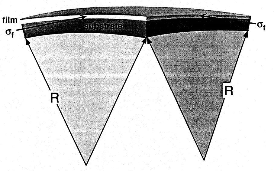
Figure n-1. Substrate curvature is produced by a thin film in a state of equibiaxial stress.
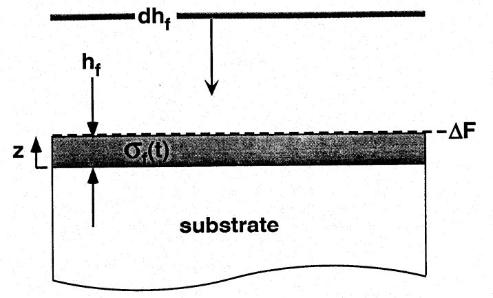
Figure n-2. Contributions to incremental changes in curvature include deposition
relaxation of the already deposited film, and surface evolution.
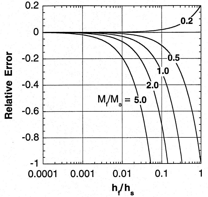
Figure n-3. The error in using Stoney’s equation when the thin film approximation is relaxed,
plotted for a range the relative film/substrate biaxial moduli.

Figure n-4. The error in using Stoney’s equation when finite deflections are accounted for.
(a) 300 µm thick substrate and (b) 100 µm thick substrate.

Figure n-5. Schematic illustration of a strip-shaped sample mounted in the springboard configuration.
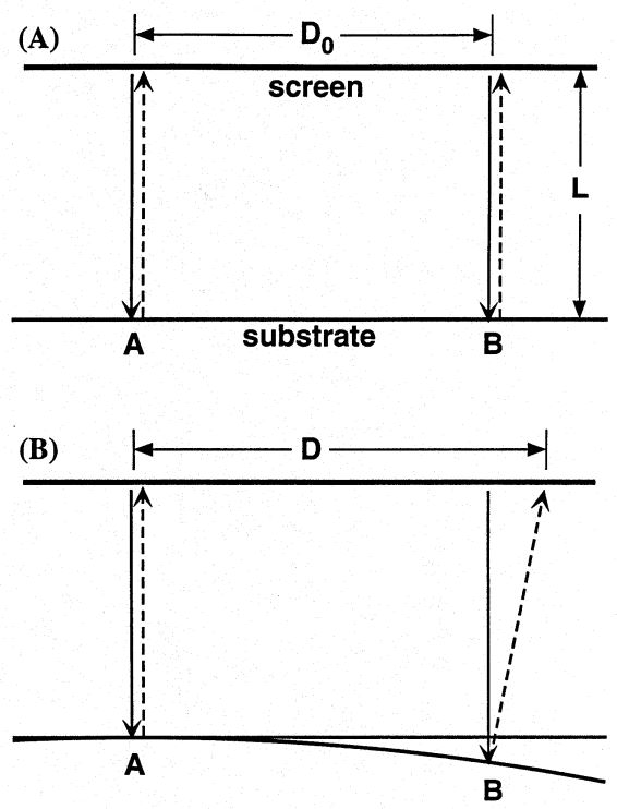
Figure n-6. The deflection of a reflected laser beam measures the local curvature of the sample.
(a) Motion of the incident beam a distance  on a flat sample moves the reflected spot an identical distance.
(b) On a curved sample,  .
.
Figure n-7. Schematic of scanning deflectometer using the rotating mirror approach.
Figure n-8. (a) The Multi-beam Optical Sensor (MOS). (B) The intensity map from the camera for a five-spot array.
Figure n-9. Unconstrained bending is allowed by mounting the sample in a “perimeter cage”.
Figure n-10. The apparent stress-thickness arising from curvature induced by a linear
temperature gradient through the thickness of a Si wafer, for various substrate thicknesses, .
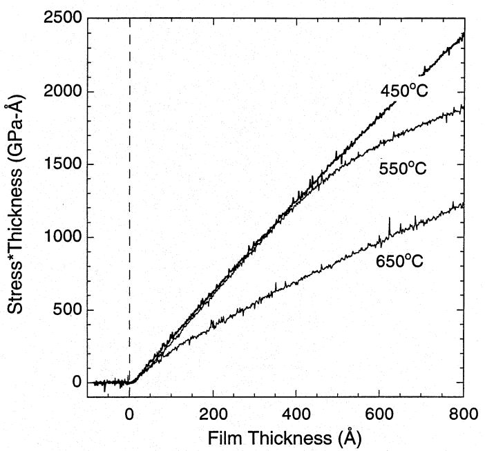
Figure n-11. The stress-thickness vs. deposited film thickness during heteroepitaxial MBE growth
of  alloys on Si at 450°C, 550°C, and 650°C. Departure
from linearity arises from the introduction of propagation of misfit dislocations.
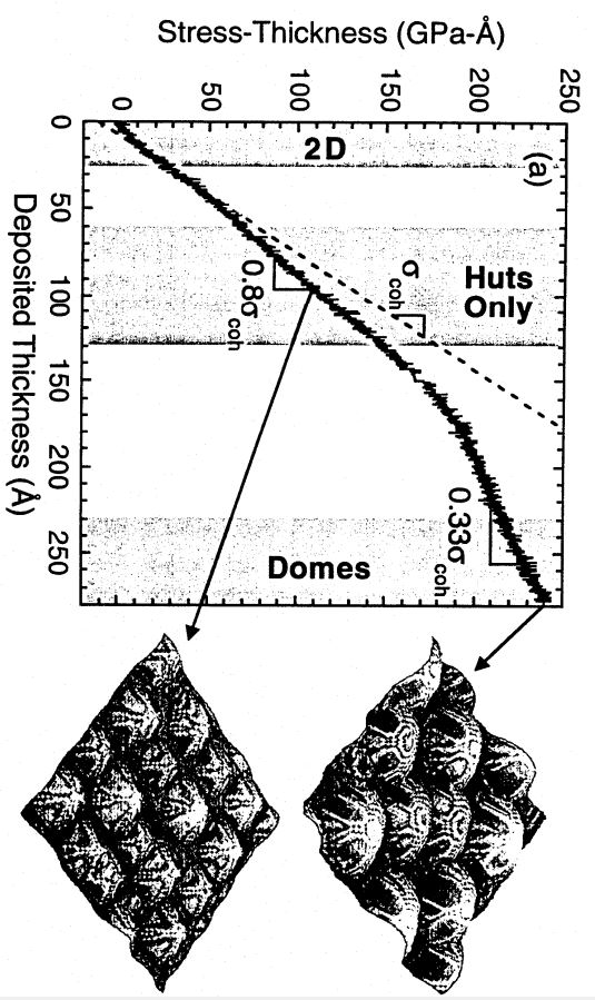
Figure n-12. The stress-thickness evolution during heteroepitaxial MBE growth of 
on Si at 755°C. Morphological regimes indicated on the figure were determined by
ex situ analysis. 2×2 µm AFM images of the hut and dome morphologies are shown.
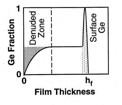
Figure n-13. Schematic illustrations of the denuded zone created in the early stages of growth by the Ge
surface segregation process. The shaded area under the Ge surface layer is equal to the shaded area
above the curve in the denuded zone.
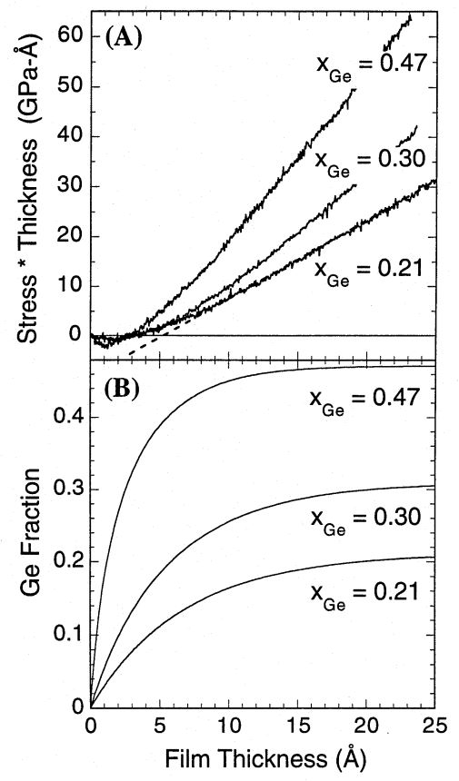
Figure n-14. (a) The stress-thickness during  MBE growth at 400°C. Note the initial
non-linear behavior. (b) The composition profile resulting from Ge surface segregation,
determined from analysis of the curvature data in (a).

Figure n-15. The curvature evolution during deposition and subsequent annealing of a Ag thin film on amorphous SiO2.
The thermal and intrinsic contributions to the measured curvature are shown explicitly.
