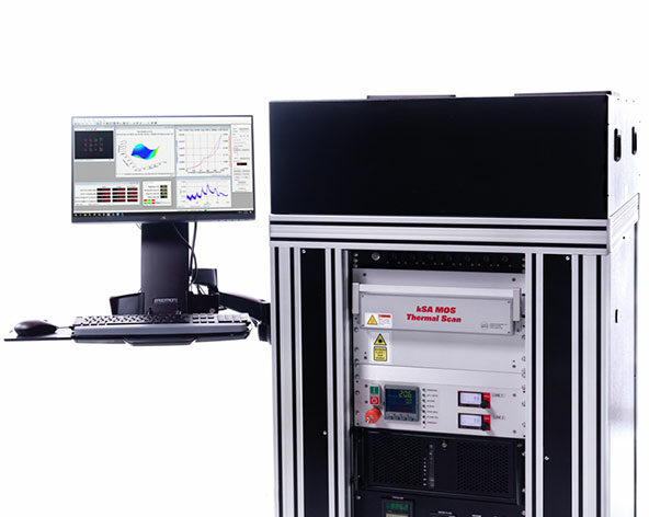
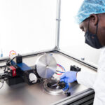
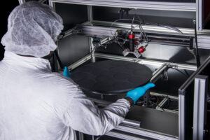
k-Space utilizes its world class metrology tools to offer in-house wafer and sample characterization. Our thin-film characterization tools can perform full wafer/sample maps of curvature, bow height, tilt, and absolute reflectivity at 660nm. We can also perform spectral reflectivity, absolute transmission, optical absorption edge, and temperature-dependent optical absorption edge measurements.
- Curvature & Bow
- Film Thickness
- Reflectivity and Transmission
- Semiconductor Optical Absorption
- Wafer Carrier Characterization
Wafer Curvature, Bow Height, and Tilt Characterization
- Standard Wafer Sizes: 2-inch, 3-inch, 100mm, 150mm, 200mm and 300mm. Wafers/samples must be mirror-like or near mirror-like surface quality (can see reflection in sample)
- Custom sizes can be measured but may require machining of custom sample holder (quoted separately)
- Scan Types:
- line scan
- Selectable area scan, up to full wafer with 5mm edge exclusion
- Scan resolution: 1um
- Maximum radius of curvature and bow height are sample size dependent. Full area scans can be performed on wafer diameters to 300mm if radius of curvature is >= 10m.
- Curvature resolution: <= 2e-5 (1/m)
- Bow height resolution: <= 0.01um
- Tilt resolution: <= 0.01 arcsec
Film Thickness Measurement
- Semi-transparent, heterostructure films (at least 1 interface, e.g. SiO2 on glass)
- Minimum film thickness of 5nm
- Need dispersion curve data on film material
- Only total film thickness measured, not individual layer thicknesses
Absolute Reflectivity and Transmission Measurement
- Both absolute reflectivity and transmission measurements made at 405nm, 532nm, and 660nm
Spectral Reflectivity Measurement
- Wavelength range: 380nm to 1700nm
- Regulated Quartz Halogen and Xe Light Sources
- Absolute reflectivity measurements can be made using in-house calibration standards over the 350nm-1100nm range with better than 0.5% absolute reflectivity accuracy
Semiconductor Optical Absorption Measurement
- Semiconductor optical absorption edge and temperature dependence of the optical absorption edge can be measured for semiconductors with band gaps in the range 0.8eV to ~3.35eV.
- Measurements can be made in high vacuum to approximately 800ºC or in a controlled atmosphere tube furnace (N2 or Ar) to 1000ºC.
MOCVD Wafer Carrier Characterization Mapping
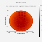
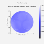
Have your K465i or EPIK 700 MOCVD carrier evaluated with the kSA Emissometer .
- Diffuse and specular reflectance maps
- UV photoluminescence maps
- Emissivity maps
Email [email protected] for more details.
