Measure and provide feedback for curvature, stress, reflectivity and growth rate to improve production processes and increase profitability with the kSA MOS.

Understanding and controlling stress in thin-film and thermal annealing processes is critical for achieving the desired optical, electronic, and mechanical properties. Many of today’s high performance devices rely on or must be designed with “built-in” stress within the individual layers for tailoring specific characteristics. However, unwanted changes in thin-film stress can be introduced at any stage of the fabrication process and may lead to a reduction in device performance as well as delamination or cracking of deposited films.
Traditional ex situ stress/strain measurement methods such as XRD or surface profiling only measure the overall stress after the process is done, but completely miss the dynamic changes in thin-film stress occurring during the process. Being able to measure the stress/strain in situ, during the process gives important insight into mechanisms and methods for controlling and targeting the overall stress induced into the sample during every step.
 Click to Enlarge
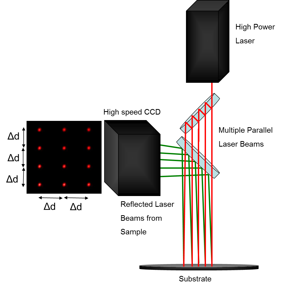
Real-Time Thin-Film Curvature and Stress in Two Directions Simultaneously
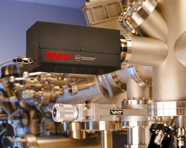
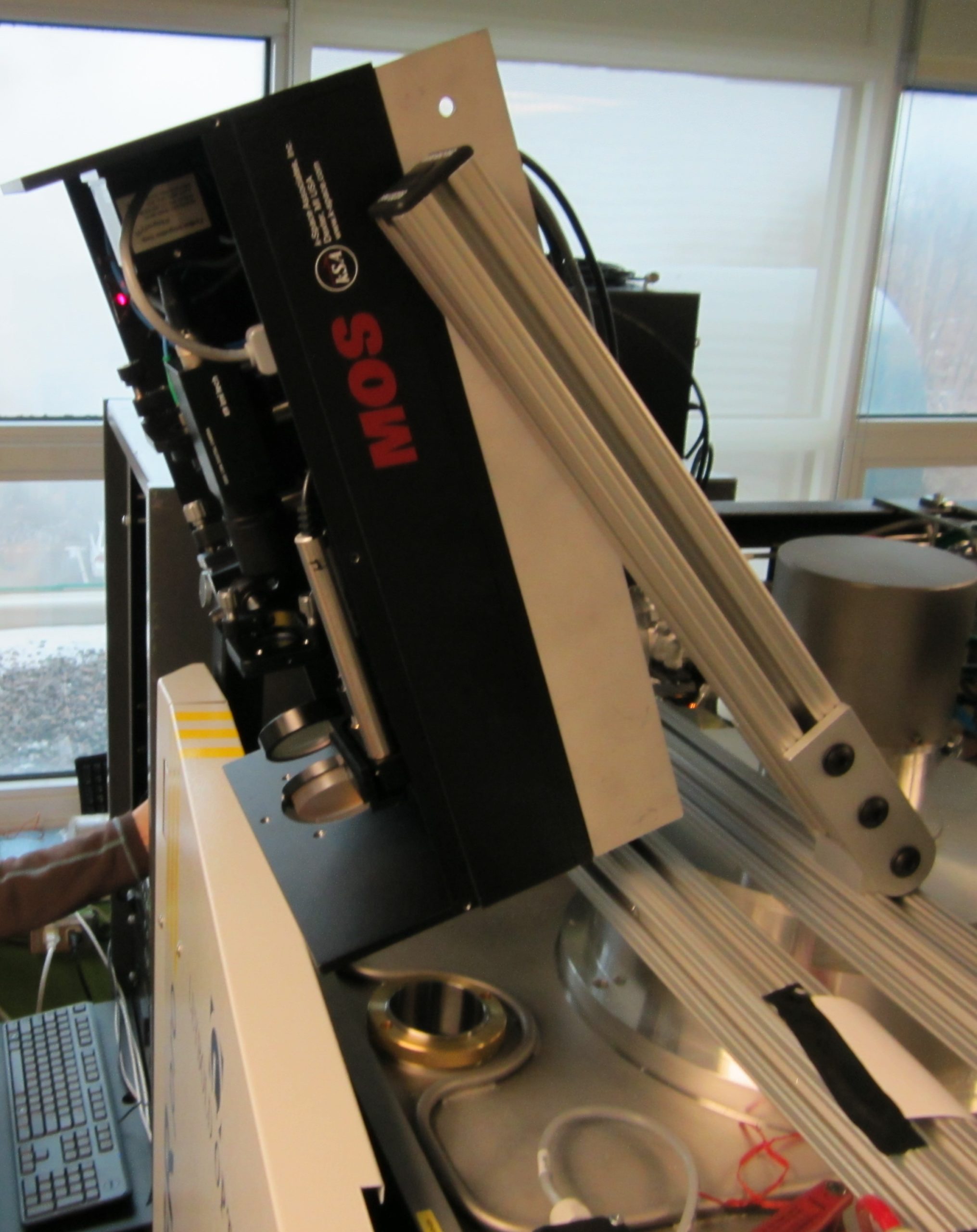
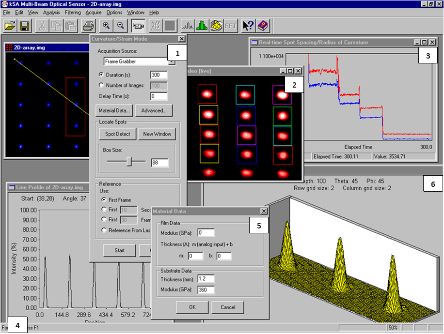
In response to a need for in situ thin-film stress measurement, kSA co-developed and patented a new, real-time stress/strain monitoring technique with Sandia National Laboratory over 15 years ago. The k-Space Multi-beam Optical Sensor (kSA MOS) uses an etalon, with highly reflective dielectric coatings on each side, that is placed at an angle to a single solid state laser beam. The incidence angle of the laser leads to multiple internal reflections within the etalon, which generates a linear array of parallel beams. These beams also pass through a second rotated etalon to produce a 2-dimensional array of beams for simultaneous 2D measurements in both x and y planes. The number and spacing of these beams can be controlled by the rotation angle of each etalon. The low power (Class 1) array of parallel beams is then reflected from the sample surface and directly imaged with a high resolution camera. During thin-film or thermal stress, the sample being imaged with the kSA MOS laser array will undergo convex or concave changes in curvature which translate into the laser spots getting farther apart (convex) or closer (concave) relative to each other on the camera. By using this wafer curvature measurement and the known geometry and material properties of the substrate and film, real-time stress is determined directly via Stoney’s equation.
 Click to Enlarge
In Situ Measurement
The kSA MOS optics are mounted directly to the vacuum or process chamber viewport and contain laser-beam array optics and camera optics with patented automatic steering mirror to ensure the laser array stays directly on the camera center. Chamber integration can be with single port (normal incidence) or dual port (specular viewports) and provides several benefits for in situ thin-film stress measurement. The kSA MOS optics are simple and stationary, requiring only minimal alignment and calibration during initial setup. Simultaneous detection and spot spacing analysis of the array makes the measurement inherently less sensitive to sample vibration compared with scanning, single beam systems. Since all the kSA MOS laser spots move together at the same frequency, sample shift or tilt is not detected as a change of curvature. Through the use of simple image processing and rapid data analysis algorithms, kSA MOS technology can easily detect micron-size changes in spot position on the camera. This translates to radius of curvature resolution in the 20-50km range; powerful enough to detect the stress induced by a single monolayer of material deposited on the substrate surface. By monitoring the entire array of beams, two-dimensional, dynamic wafer and thin-film curvature and stress profiles can be obtained with enough speed necessary for real-time measurement and process control.
 Click to Enlarge
Applications
The kSA MOS thin-film measurement tool is currently being used for in situ stress monitoring and control at leading R&D and full production facilities worldwide. Applications include metal film sputtering, high performance dielectric and filter coatings (PVD), glass panel processing, 300mm semiconductor IC processing, thin-film battery research, epitaxial layer growth during MBE and MOCVD, and thermal stress monitoring during annealing. Don’t wait until it’s too late – control your thin-film or thermal stress in real time with kSA MOS!
Software Capabilities
- Complete data acquisition and analysis control.
- Automatic laser spot detection.
- Automatic camera exposure control to ensure no saturation of detector as surface reflectivity changes.
- Real-time plotting of intensity, reflectivity, differential spot spacing, stress-thickness product, strain, and radius of curvature.
- Data acquisition modes:
- Focus mode: for facilitating laser alignment and optics focusing by simultaneously monitoring the image and a line profile of the laser spot array.
- Curvature/Strain Mode: An arbitrary number of laser spots, user configured, are tracked simultaneously; yielding time-resolved radius of curvature measurements, mean differential spot spacing, stress, reflectivity, and intensity. The mean differential spot spacing is used to calculate time resolved stress or stress thickness product using material parameters.
- For time-resolved acquisition modes, a delay time between image acquisitions, may be selected.
- External triggering can be used to time data acquisition with external events or substrate rotation.
- Analysis Capabilities:
- Line profile for accurate determination of beam profiles.
- Radius of curvature and strain analysis. User input of physical geometry and substrate parameters yields calculation of radius of curvature, stress-thickness product, or relative stress as a function of time, temperature, or other user configurable input. Alternatively, simple centroid position and spot separation distance may be plotted.
- Data storage in ASCII, Excel or binary file formats facilitate alternative data analysis by user.
- User-friendly Windows 10-standard environment with extensive error checking and file handling. Data storage in ASCII, Excel or binary file formats facilitate alternative data analysis by user. Direct printing of images or graphics using currently loaded Windows printer drivers. Cut-and-paste directly to clipboard, or into other applications such as MS Word or PowerPoint.
- High-quality 2D and 3D graphics for data display. Numerous image and graphics editing capabilities, including false coloring using pre-loaded or user-defined color palettes, and label editing. Transport of graphics directly to Windows clipboard or exported to Windows Metafile, Tiff or Bitmap format.
- Complete TCP/IP interface for custom, real-time data transfer and program control. Ability to write to an SQL database. Analog and Digital I/O capability with optional hardware (quoted separately).
Optional Software
kSA MOS Analysis Only Software Sentinel Key (M-AOS)
M-AOS option is an analysis-only software sentinel key that allows complete kSA MOS functionality, with the exception of data acquisition. It is designed for users who want to perform post acquisition, display, processing and analysis away from the laboratory.
Growth Rate Monitor Option for kSA MOS Software (MOS-GM)
As an add-on to the standard MOS software, the MOS-GM software option offers:
- Reflected intensity oscillation data recorded during growth can provide accurate growth rate and optical constant determination for semi-transparent films.
- Real-time update of current n, k, deposition rate, and standard deviation of these values.
- Ability to generate a thin-film deposition recipe, so multiple layers can be properly fit in real-time. Each layer in the recipe will have a user-estimated n, k, and G value. Each layer can be triggered via a time-based kSA MOS software recipe or an external trigger signal (with the purchase of additional A/D communications options or via the integrated TCP/IP protocol.)
- Optional ability to output growth rate, thickness, n, and k to analog output channels for input into process control system.
References
View All ReferencesEffect of Crystallite Geometries on Electrochemical Performance of Porous Intercalation Electrodes by Multiscale Operando Investigation
Yuting Luo, Yang Bai, Aashutosh Mistry, Yuwei Zhang, Dexin Zhao, Susmita Sarkar, Joseph V. Handy, Shahed Rezaei, Andrew Chihpin Chuang, Luis Carrillo, Kamila Wiaderek, Matt Pharr, Kelvin Xie, Partha P. Mukherjee, Bai-Xiang Xu & Sarbajit Banerjee
Growth design for high quality AlxGa (1− x) N layer with high AlN-fraction on Si (1 1 1) substrate by MOCVD
Abheek Bardhan, Srinivasan Raghav
Reconfiguration of Amorphous Complex Oxides: A Route to a Broad Range of Assembly Phenomena, Hybrid Materials, and Novel Functionalities
Divya J. Prakash,Yajin Chen,Mengistie L. Debasu,Donald E. Savage,Chaiyapat Tangpatjaroen,Christoph Deneke,Angelo Malachias,Adam D. Alfieri,Omar Elleuch,Kaddour Lekhal,Izabela Szlufarska,Paul G. Evans,Francesca Cavallox
Wafer-Scale Electroactive Nanoporous Silicon: Large and Fully Reversible Electrochemo-Mechanical Actuation in Aqueous Electrolytes
Manuel Brinker and Patrick Huber
Silicon Contamination of the Praseodymium Doped Ceria Oxygen Surfaced Exchange Coefficient
Yuxi Ma and Jason D. Nicholas
Negative Thermal Expansion HfV2O7 Nanostructures for Alleviation of Thermal Stress in Nanocomposite Coatings
Guan-Wen Liu, Yuwei Zhang, Melonie P. Thomas, Ahamed Ullah, Matt Pharr, Beth S. Guiton, and Sarbajit Banerjee
