Increase quality with controlled deposition, stress monitoring and RHEED analysis to optimize your physical vapor deposition (PVD) processes.
Physical Vapor Deposition (PVD) is the most widely used technology for depositing materials as a thin film onto a host substrate. From metals, to semiconductor materials, to the most complicated optical film stacks, PVD is the most common deposition method. PVD is used in the manufacture of a wide range of goods, including semiconductor devices, aluminized PET film for balloons and snack bags, optical coatings and filters, coated cutting tools for metalworking and wear resistance, and highly reflective films for decorative displays.
PVD tools have also been developed for the fabrication of extremely thin films, i.e. films only nanometers in thickness. PVD deposition tools can deposit monolayers of virtually any material, including materials with melting points up to 3500 °C. There are variants of the PVD process whereby the method for generating the physical vapor is different, but all processes take place in a vacuum chamber of some type. PVD, like other deposition processes, benefits from in situ process monitoring.
The PVD coating method involves a purely physical process. The three most common processes are 1) plasma sputtering, 2) pulsed laser deposition, and 3) e-beam evaporation. The film materials are transferred via various methods from some starting ‘target’ with subsequent condensation onto the host substrate.
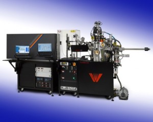
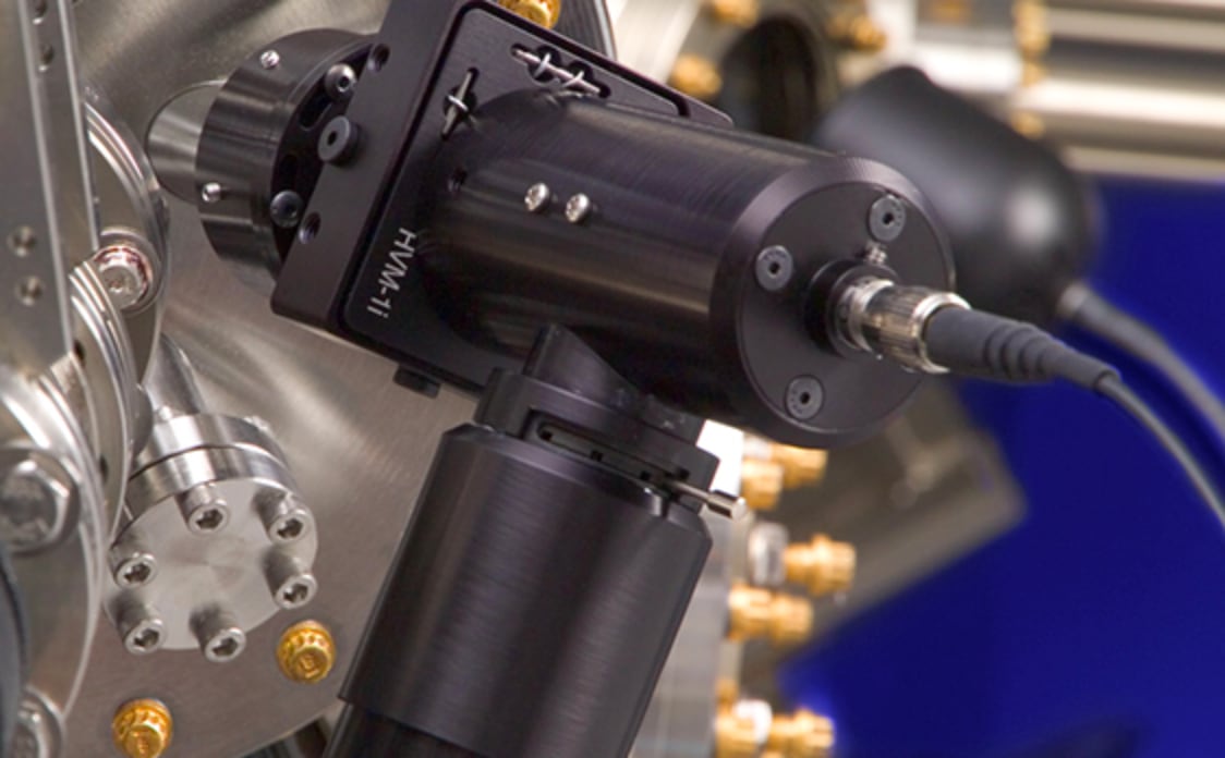
RHEED analysis is a proven technique for PVD applications utilized in R&D and full production facilities worldwide. Being able to analyze the surface structure and morphology via electron diffraction on a phosphor RHEED screen with the kSA 400 RHEED system provides real-time film growth information. Growth rate, surface structure and texture, and lattice spacing/strain are easily determined using the kSA 400 RHEED system.
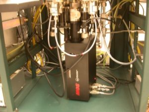
Uncontrolled and unevaluated stress in thin films can cause serious problems with device performance and production yield. Being able to measure the stress in real-time during the growth process provides insight into the stress mechanisms and allows for optimization or minimization of the film stress. This leads to improved device quality.
The kSA MOS is proven to provide this insight and feedback in a wide range of PVD and sputtering applications in both R&D and full production facilities. It has the ability to measure and provide feedback for curvature, stress, reflectivity and growth rate to improve production processes and increase profitability.
