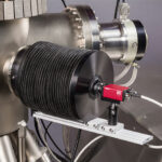
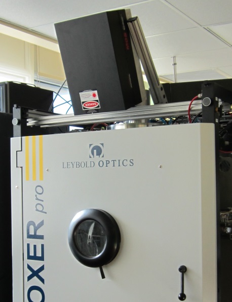
Advanced optical device fabrication calls for advanced technologies like in situ tools for feedback control of key evaporation parameters such as stress, curvature and bow in real-time.
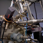
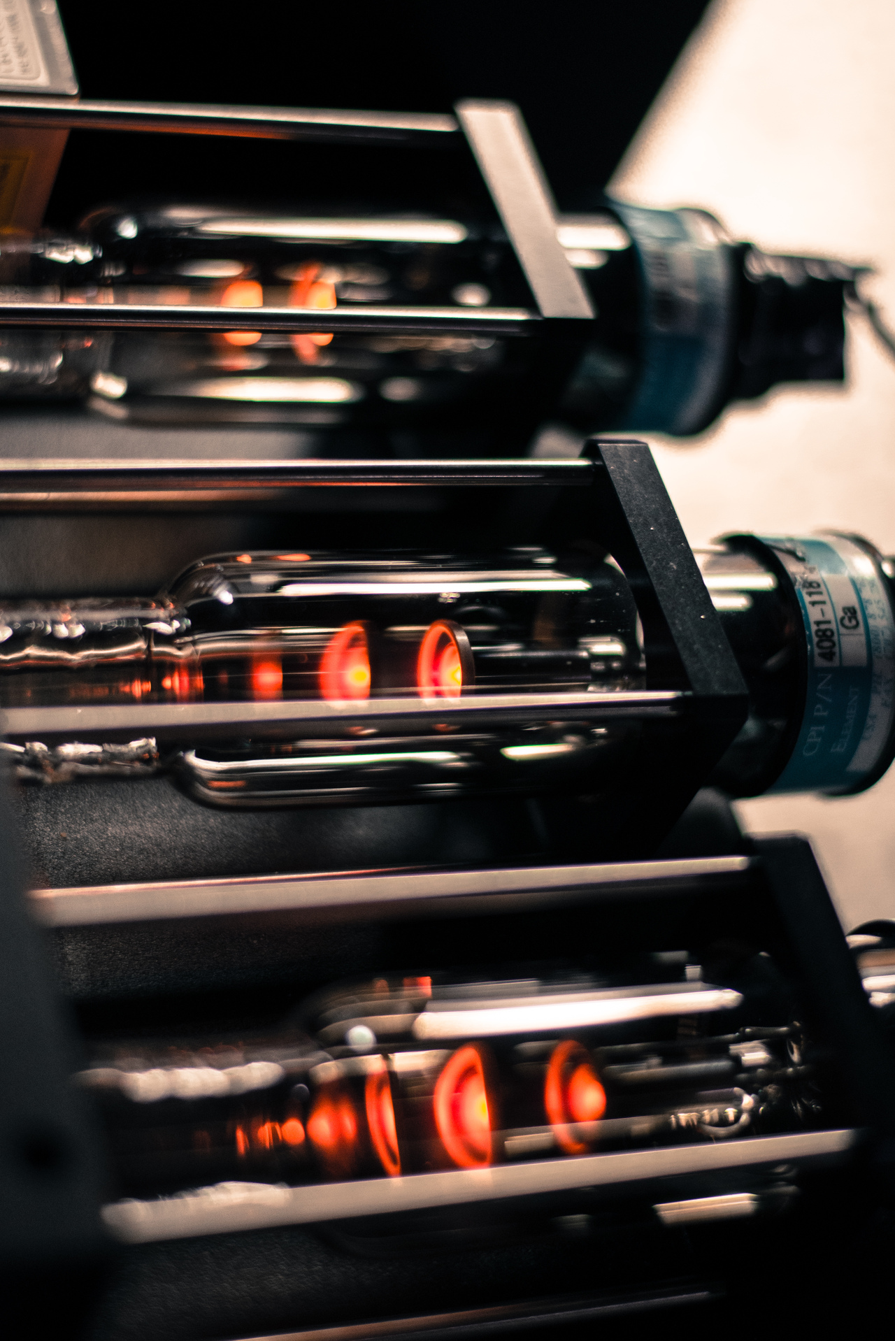
E-beam evaporation utilizes a high energy electron beam to bombard the source material target, heating the target in high vacuum to a high vapor pressure, resulting in atomic or molecular diffusion of the material to the substrate, where it is deposited by condensation. As with sputtering or PLD, important real-time information related to film characteristics at the surface can be obtained with the right tools.
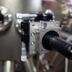
By using kSA MOS, multi-layer stress formation can be monitored and controlled during the most advanced optical thin film device fabrication. Being able to measure the stress in real-time during the growth process provides insight into the stress mechanisms and allows for optimization or minimization of the film stress. This leads to improved device quality.
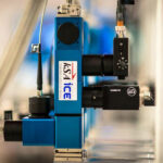
kSA MOS has the ability to measure and provide feedback for curvature, stress, reflectivity and growth rate to improve production processes and increase profitability.