Real-time absolute temperature measurement of standard semiconductor substrates like GaAs, InP, and Si, as well as wide bandgap substrates transparent in the IR (including GaN, SiC, ZnO, AlN, Ga2O3 and SrTiO3). Go where pyrometers can’t!

The kSA BandiT is a non-contact, non-invasive, real-time, absolute wafer and thin-film temperature monitoring tool used during thin-film deposition and thermal processing. Using the temperature-dependent optical absorption edge inherent in semiconductor materials, kSA BandiT provides semiconductor temperature monitoring in ranges that pyrometers cannot measure: substrates transparent in the infrared (including GaN, SiC, ZnO, AlN, Ga2O3 and SrTiO3), as well as low temperature monitoring, e.g. low temperature GaAs, InP, and Si deposition. This includes room temperature wafer measurements. Furthermore, kSA BandiT is immune to changing viewport transmission, stray light, and signal contribution from substrate or source heaters, all sources of measurement error for pyrometers.
 Combined with its patented blackbody emission monitor, kSA BandiT has the ability to monitor the full range of temperatures for most substrate materials, including low band-gap substrates and metal films. Finally, because kSA BandiT uses a solid-state spectrometer, real-time film thickness and surface roughness can also be measured.
 Click to Enlarge
Band Edge Temperature/Thermometry (BET)
The most common application of the kSA BandiT tool is for direct substrate temperature measurement. By measuring the position of the substrate absorption edge, the absolute temperature of the wafer can be determined. This absorption edge, which is directly proportional to the band gap of the material, is temperature dependent. It is this temperature dependence that we rely on to determine the wafer temperature. A solid-state spectrometer is used to acquire either diffusely reflected, or transmitted light from the wafer. This spectra is then analyzed in real-time by the kSA BandiT software, fitting to the absorption edge, and determining the absolute wafer temperature from the position of the absorption edge.
 Click to Enlarge
Blackbody Temperature Measurement
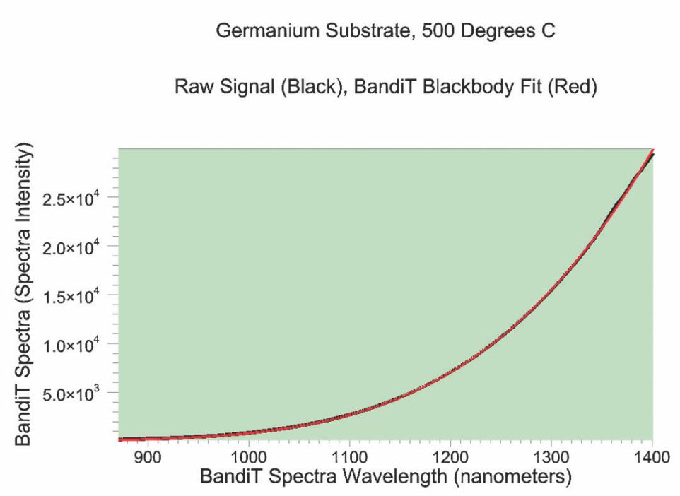
In addition to kSA’s patented band edge temperature measurement, BandiT offers a complimentary measurement technique, blackbody temperature measurement. This approach, also patented by k-Space, fits the radiation emitted from the wafer to Planck’s equation. In this approach, the emissivity of the wafer can be changing, without affecting the temperature measurement. This is because it is the functional shape of the blackbody spectra, not its amplitude, that dictates the temperature of the emitting material. This is unlike pyrometry, which relies solely on the absolute signal level in a given (small) wavelength range. The kSA BandiT blackbody temperature measurement is typically used when the band edge of the material cannot be measured. This occurs typically when looking at a non-semiconductor substrate, a heavily doped substrate, or a very narrow band gap substrate (e.g. Ge or InAs). The blackbody temperature measurement technique typically has a lower limit in temperature of ~ 250 °C, due to limited emitted radiation at low temperatures.
Film Thickness and Roughness Measurement
Because a solid-state spectrometer is used with the kSA BandiT system, the full diffuse spectra is obtained. This spectra contains a wealth of information in addition to the material absorption edge. By analyzing the below gap interference fringes, the total film thickness can be very accurately determined. By analyzing the above gap scatter signal, changes in roughness can be easily monitored. Combined with real-time temperature measurement, kSA BandiT offers a very powerful in situ monitoring tool for your thin-film deposition and processing needs.
 Click to Enlarge
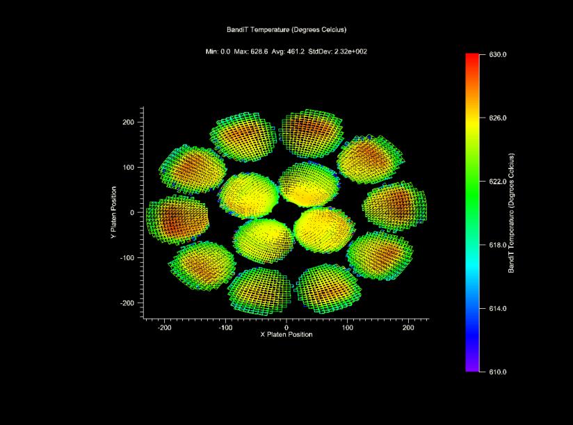
Multiwafer and Full Platen Scan Capability
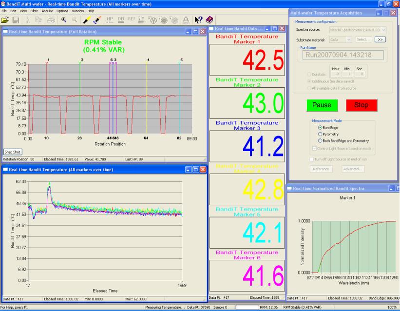
kSA BandiT can be configured to synchronize to substrate rotation. For production applications, or where multiwafer platens are used, the kSA BandiT MW (MultiWafer) system allows you to monitor the temperature of all wafers on the platen. Markers can be placed where you are interested in temperature measurement, for example at wafer centers and edges.
 Click to Enlarge
If you desire full platen maps of temperature, the kSA BandiT Platen Scan option allows you to control the position of the BandiT detector head, yielding wafer temperature maps of the entire platen. A computer-controlled motor on the kSA BandiT head steps to every desired radius position on the platen, and data is taken synchronously during rotation at every radial position. Detailed temperature maps and template analysis statistics then allow you to adjust heater zone tuning ratios, determine hot or cold spots in the platen pockets, etc.
 Click to Enlarge
Temperature Capabilities
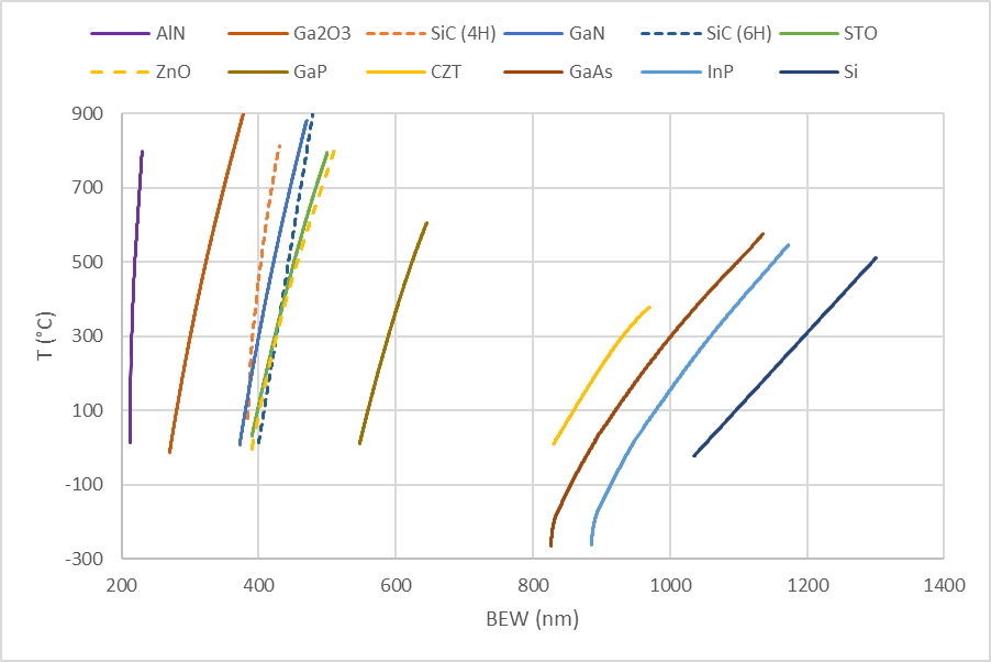
kSA BandiT can measure substrate temperatures from > 1000C all the way down to ~ -250C. The graph at right shows the temperature vs band gap dependence (as determined using kSA BandiT) for a variety of semiconductor materials. Note that the slope of this dependence gets steeper as you go from small to wide bandgap materials. Note that GaAs and InP band gap dependence has been taken all the way down to cryogenic temperatures.
What You Get With a kSA BandiT System
 Click to Enlarge
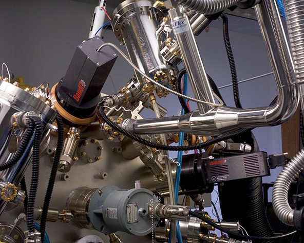
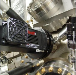
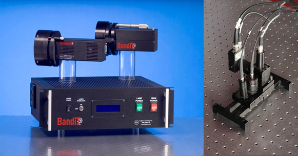
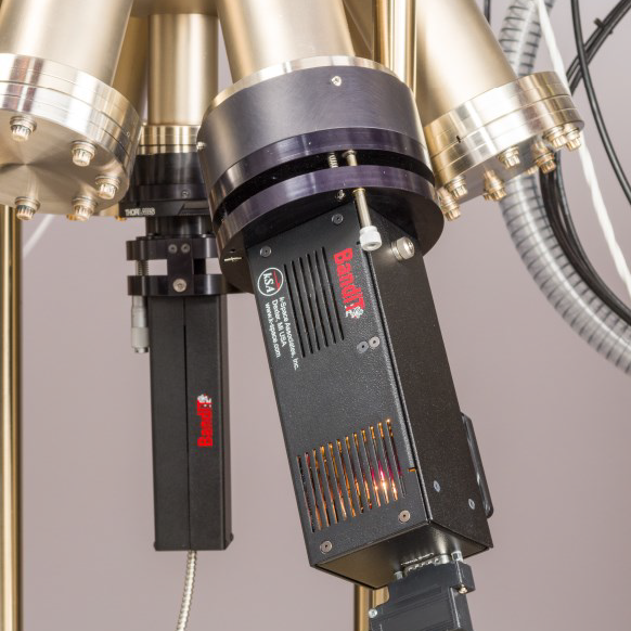
The kSA BandiT system comes in several different flavors, depending on what type of growth or materials processing chamber you have. Our most common kSA BandiT configuration includes a light source optics, a detector optics head, and a 19” rack mount electronics controller. In many cases, e.g. high temperature MBE growth, the substrate heater can be used as the light source, and a light source optics head is not needed. In most MOCVD applications, the viewport to sample distance is relatively short and the optical access is limited. As such our optics heads for most MOCVD reactors are small, and integrate a light source and detector into a single head.
Whatever your chamber configuration, we’re confident we can supply a kSA BandiT system for your in situ metrology needs. We look forward to hearing from you about your thin-film and wafer temperature measurement needs!
kSA BandiT data acquisition and analysis software is a full featured package that controls and monitors the light source, spectrometer(s), and all data I/O, as described in the spec sheet. Hardware interface is through a single USB connection to the BandiT rack.
The customizable user interface offers real-time display of temperature, thickness, surface roughness, growth rate, processed spectra and curve fitting routines. In addition to these features are the following:
- Complementary analysis only software license for post-deposition/acquisition analysis. Data storage in ASCII, Excel, or binary file formats facilitates alternative data analysis by user.
- Copies graphics directly to Windows clipboard or exports directly to .wmf, .bmp, .png, or .tif formats. Export data to .xls and .txt formats.
- TCP/IP interface for custom, real-time data transfer and program control.
- Ability to write data in real-time to an SQL database.
- Analog and digital data I/O capability.
- User-configurable window layout.
Patented Technology
 Click to Enlarge
The kSA BandiT metrology tool includes the following patented technologies:
- Patented methodology for using the measured semiconductor band edge to determine the temperature of semiconductor substrates.
- Patented methodology for fitting the measured sample emission spectrum to Planck’s equation for blackbody radiation, yielding the absolute temperature of the sample.
- Patented methodology for measuring film temperature, film thickness, and surface roughness on near infrared (NIR) transparent substrates.
These technologies are covered by US patents 8,786,841, 8,282,273, and 7,837,383.
References
View All ReferencesGrowth of PbTe Nanowires by Molecular Beam Epitaxy
Sander G. Schellingerhout, Eline J. de Jong, Maksim Gomanko, Xin Guan, Yifan Jiang, Max S.M. Hoskam,
Sebastian Koelling, Oussama Moutanabbir, Marcel A. Verheijen, Sergey M. Frolov, Erik P.A.M. Bakkers
Consideration of the Intricacies Inherent in Molecular Beam Epitaxy of the NaCl/GaAs System
Brelon J. May, Jae Jin Kim, Patrick Walker, William E. McMahon, Helio R. Moutinho, Aaron J. Ptak, David L. Young
Molecular Beam Epitaxy of GaAs Templates On Water Soluble NaCl Thin Films
Brelon J. May, Jae Jin Kim, Patrick Walker, Helio R. Moutinho, William E. McMahon, Aaron J. Ptak, David L.Young
AlInAsSb Avalanche Photodiodes on InP Substrates
Kodati, S. H.; Lee, S.; Guo, B.; Jones, A. H.; Schwartz, M.; Winslow, M.; Pfiester, N. A.; Grein, C. H.; Ronningen, T. J.; Campbell, J. C.; Krishna, S.
The Microstructural and Stress Evolution in Sputter Deposited Ni Thin Films
Thomas Koenig, Zhaoxia Rao, Eric Chason, Garritt J. Tucker, Gregory B. Thompson
Large Tunable Bandgaps in the InAs/AlAs Strain-compensated Short-period Superlattices Grown by Molecular Beam Epitaxy
Jinshan Yao, Rui Pan, Wenyang Wang, Chen Li, Baile Chen, Hong Lu, and Yan-Feng Chen
