Open the door to a quantitative approach to wafer carrier characterization in the MOCVD production environment.
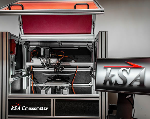
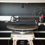
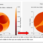
The kSA Emissometer is designed to quickly and easily generate high-resolution diffuse and specular reflectance and total emissivity maps of MOCVD carriers. Carrier emissivity variation means temperature non-uniformity, which can lead to reduced device yield and possibly complete growth run failure. With the kSA Emissometer, emissivity changes can be tracked to determine carrier end-of-life, without wasting growth runs. The kSA Emissometer also detects unwanted residual deposits after baking, and easily identifies carrier surface defects, scratches, microcracks and pits that are not visible to the eye.
The kSA Emissometer is used for:
- Determination of the quality of the carrier bake after the deposition run. Yields a “Go-no-go” decision on the suitability of a particular carrier for the next production run.
- Quantitative determination of real surface emissivity and the necessary temperature set-point adjustments for a particular wafer carrier post-bake.
- Presence and severity of the microcracks in the SiC coating. Decision to retire the wafer carrier at the end of its useful lifetime.
- Qualification of the wafer carrier vendors, via examination of the emissivity uniformity over the carrier and within the batch of carriers. Incoming quality control (QC) of the new wafer carriers.
- Prevention of wasted MOCVD growth runs.
For more information see the Product Specification Sheet →
Emissivity, Specular Reflectance, and Diffuse Reflectance
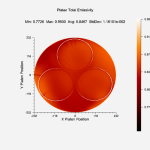
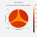
Both a diffuse reflectance and specular reflectance head scan together as the carrier rotates, producing a full map of the carrier’s diffuse reflectance, specular reflectance, and total emissivity. Measure with a user-selectable source wavelength of either 660nm or 940nm. Specular reflectance and diffuse reflectance maps build as the kSA Emissometer scans and the full carrier emissivity map is available at completion of the scan.
Scanning
Scan carriers up to 700mm in diameter in approximately 10 minutes depending on carrier size and user-selected scan resolution. An easy to use interface allows for customizing the scan resolution and scan area. The design allows for easy loading and unloading of carriers as well as simple computer control designed for operator or engineer use.
Data Display and Analysis
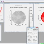
The kSA Emissometer integrated software allows for in depth analysis of the carrier diffuse reflectance, specular reflectance, and emissivity data. Statistical analysis of the carrier’s webs and pockets (both summary and individual data) is immediately available at the end of each scan. Zoom in on user selected areas in your carrier emissivity profile to take a closer look at the scan. Modify the plot parameters to best depict the carrier defects. Data is easily exportable for further analysis.
