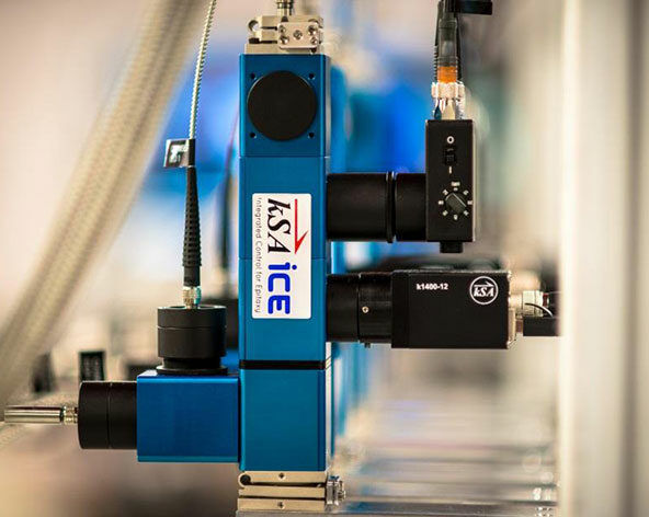
The k-Space Integrated Control for Epitaxy system (ICE) measures thin-film temperature, reflectivity, thickness, growth rate, stress and curvature. A modular in situ metrology tool designed for today’s MOCVD and MBE reactors. Each system is custom configured based on the modules that the user needs for their measurement, chamber, and materials.
The k-Space Integrated Control for Epitaxy system (ICE) is a modular in situ metrology tool designed for today’s MOCVD and MBE reactors. By integrating various measurement modules into a single optics head, the kSA ICE metrology system can measure real-time temperature, reflectivity, growth rate, film thickness, substrate curvature, and film stress.
It combines kSA MOS, and kSA RateRat Pro patented technologies, along with an Emissivity Corrected Pyrometry (ICE-ECPR) module. The kSA ICE modular design allows the user to select the modules based on what they want to measure with their kSA ICE system. When ordering, some users keep other modules in mind for future expansion.
The kSA ICE tool can handle wafer-resolved measurement for rotation speeds up to 1,500 RPM. One of the many advantages of kSA ICE is that it fits in tight spaces and measures multiple thin-film parameters in one device.
The user selects the attributes that need to be measured, and k-Space will configure a tool with the appropriate modules specifically for you. k-Space prepares a custom quote for each tool based on measurement needs, deposition method, chamber configuration, and materials.

Keep cool while gaining insight into your MOCVD or MBE process, maximizing device performance, and limiting process variation to increase yields with kSA ICE!
For more information see the ICE for MOCVD Product Specification Sheet →
For more information see the ICE for MBE Product Specification Sheet →
The kSA ICE can incorporate three temperature measurement modules.
 Click to Enlarge
Emissivity Correcting Pyrometry Module (ICE-ECPR):
The kSA ICE ECPR module uses a photodiode to measure the collected blackbody radiation intensity of a sample at a specified wavelength and integrates the measured signal into standard pyrometry equations to determine temperature. The system determines surface reflectance in real-time via an LED at the same measurement wavelength and uses this data to correct the surface emissivity to provide accurate temperature measurement for temperatures > 450 ºC.
 Click to Enlarge
SpectraTemp Calibrator Module (ICE-SPECT):
The kSA ICE SpectraTemp Calibrator module measures the spectral radiation signature of a sample over a wide wavelength range, and then it fits the curve of the response in real-time to Planck’s equation to determine absolute temperature. This patented technique is self-calibrating — it does not require a temperature reference like pyrometry does; you can use it in situ to calibrate the kSA ICE ECPR module at any time. This system measures temperatures that are typically greater than 500 ºC on bare wafers or platen.
For more information please see our Blackbody Temperature Measurement Technology Note.
 Click to Enlarge
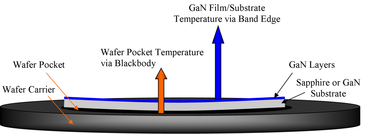
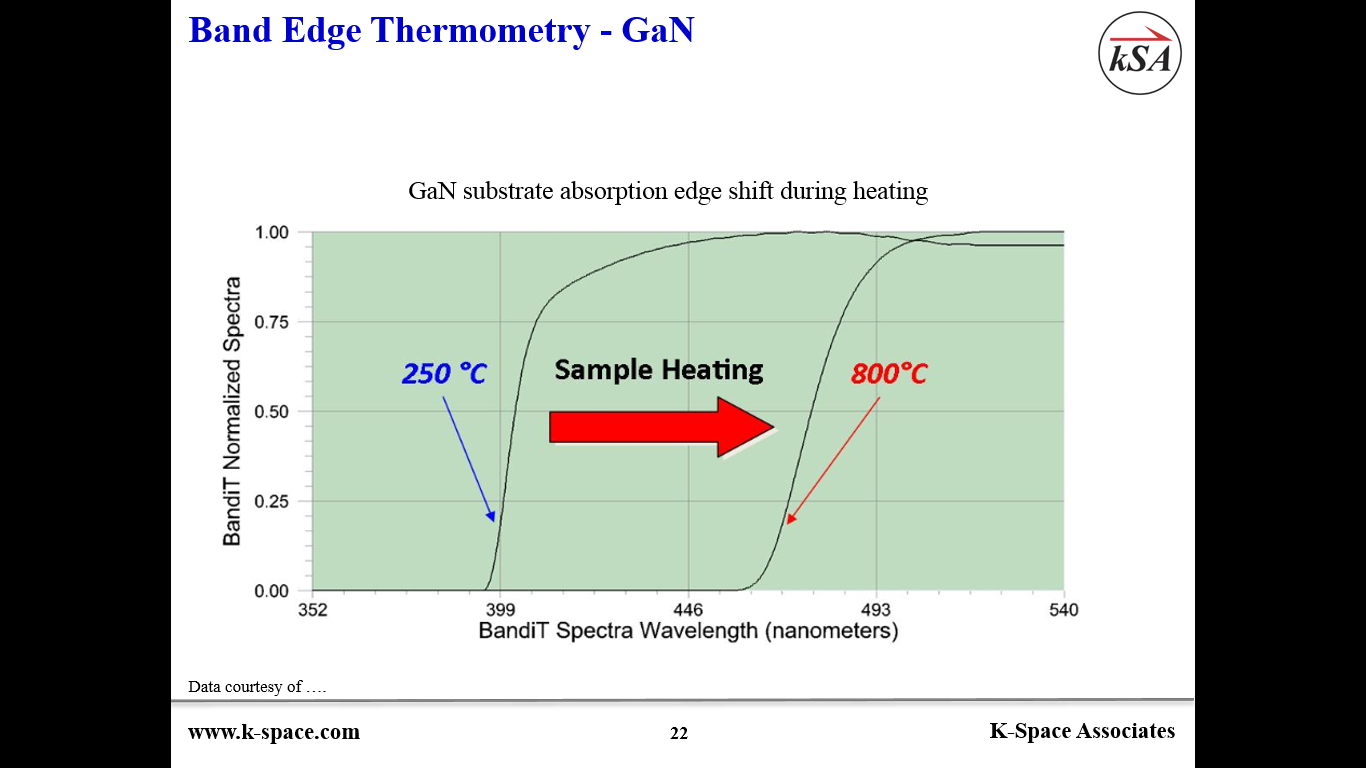
Band Edge Module (ICE-BE):
k-Space has adapted the patented technology of the kSA BandiT to enable the kSA ICE system to monitor band edge temperature. The kSA BandiT measures the temperature-dependent semiconductor optical absorption edge (band gap dependence on temperature) and uses k-Space calibration files to determine absolute film/substrate temperature (not pocket temperature). For example, using a spectrometer over the range of 350- 600 nm and a Xenon light source, the kSA ICE–BE option measures absolute GaN film or GaN/SiC substrate temperature via band-edge thermometry for direct InGaN MQW temperature and LED emission wavelength control.
For more information please visit our kSA BandiT page.
 Click to Enlarge
Measure Film Thickness, Growth Rate, and Optical Constants (n and k)
Reflectivity Module (ICE-R)
The ICE Reflectivity module is based on the kSA RateRat Pro technology. It uses a laser or LED in combination with a high-speed photodetector to monitor and fit the surface reflectivity, measuring real-time film thickness, growth rate, and optical constants (n, k). The module achieves real-time capability through a proprietary algorithm that continuously updates the optical constants of the film, derived from a least-squares fit to the optical reflectivity curve. This enables the film grower to have a continuous record of the progress of the film growth during its deposition, including all the critical parameters that are needed to characterize film quality and uniformity. Users can generate a thin-film deposition recipe and apply it to multiple layers so that they can be properly fit in real-time. The system can trigger each layer via an external trigger signal or via a time-based activation. Using a 660 nm laser, the kSA ICE-R can measure a GaN film thickness with the accuracy of ±1% after ~ 120 nm of growth.
For more information on reflectivity-based film thickness, growth rate, and optical constant measurement technologies, please visit our kSA RateRat Pro page.
Emissivity Corrected Pyrometry and Reflectivity Module (ICE-ECPR)
In addition to the capabilities mentioned for temperature measurement, the emissivity corrected pyrometry and reflectivity module also offers 960 nm LED reflectivity measurement and subsequent growth-rate and film-thickness determination at this wavelength. There is also an optional LED-based reflectivity ECPR module to provide additional wavelengths.
Band Edge Module (ICE-BE)
In addition to the capabilities mentioned for temperature measurement, the kSA ICE band edge module collects diffusely scattered light with a spectrometer and analyzes the below-gap spectral interference fringes to determine film thickness and growth rate in real-time during film deposition.
For more information on spectral interference film thickness and growth rate measurement technology, please visit the kSA BandiT page.
 Click to Enlarge
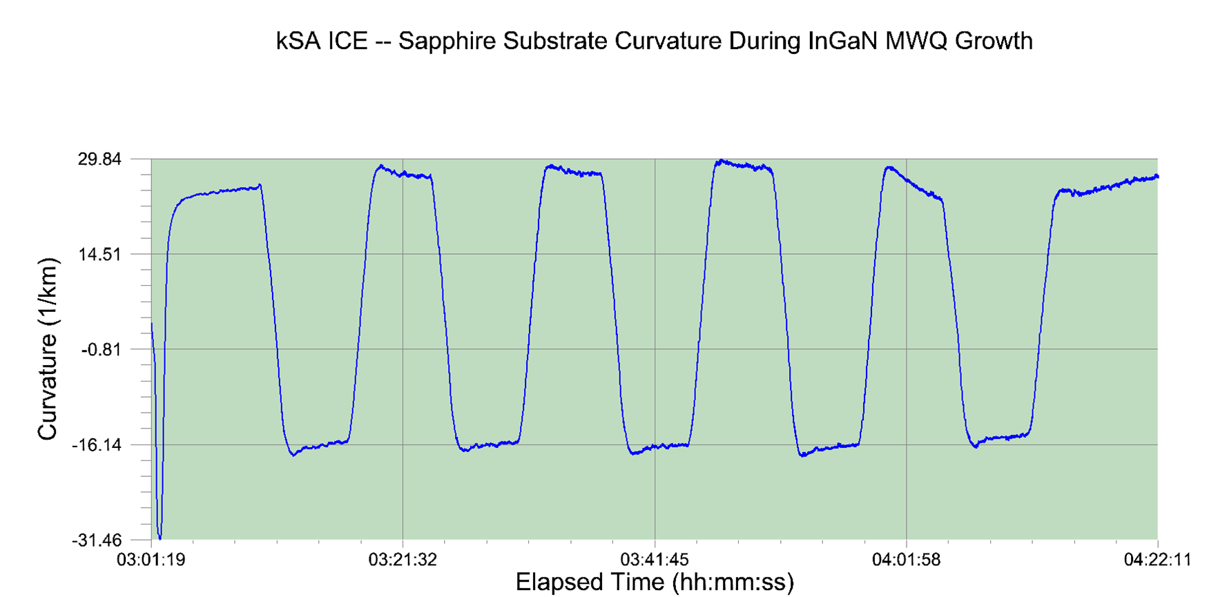
Multi-Beam Optical Sensor (ICE-MOS)
The kSA ICE system uses the patented kSA Multi-beam Optical Sensor (MOS) curvature/bow measurement technology to measure the substrate curvature with a 1D array of parallel laser beams, detecting changes in laser spot spacing caused by film or thermal stress via a camera. This is a patented wafer curvature stress measurement technology. The kSA ICE-MOS module can measure curvature from 820/km (concave) to -1640/km (convex). Complete insight into the GaN and SiC growth process for HBLED and RF power devices is now possible by optical monitoring of film stress during growth.
For more information on film stress, wafer curvature, and wafer bow measurement technology, please visit our kSA MOS page.
 Click to Enlarge
The kSA ICE system is ideally suited to provide real-time feedback to process control systems via a TCP/IP interface or analog I/O channel. Proven hardware designs are in use on today’s commercial R&D and production MOCVD and MBE systems available from Veeco, Aixtron, Taiyo Nippon Sanso, Structured Materials, and many others. Gain insight into your MOCVD or MBE process, maximize device performance, and limit process variation to increase yields with a kSA ICE!
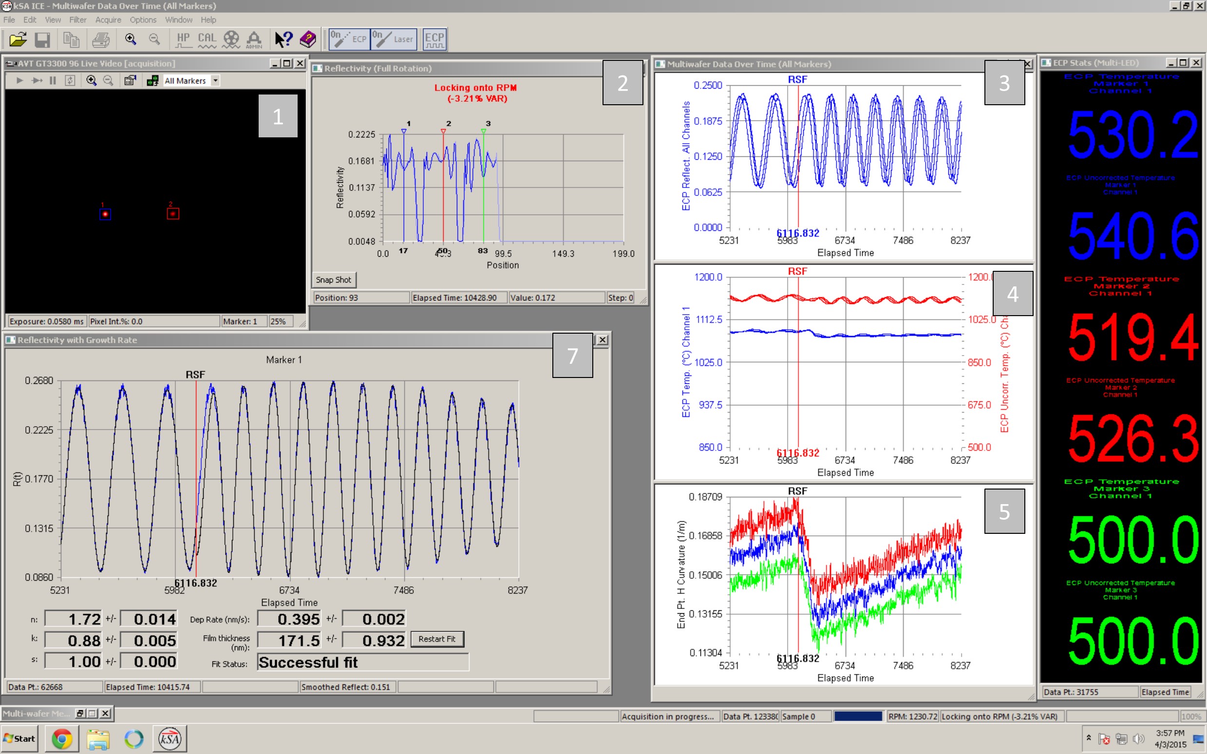
The kSA ICE software utilizes the Windows-standard operating environment with extensive error checking and file handling. Typical features are following, based on your configuration:
- Utilizes signal intensity changes in the wafer and carrier to visually trace and define wafer positions during rotation. The user is able to accurately place measurement “markers” at any position to enable real-time monitoring. Wide markers are available when averaging is desirable.
- Multi-wafer acquisition for full real-time integration and display of all pertinent acquisition parameters, at all marker positions (up to 20 markers).
- Capable of dynamically adjusting the laser and/or detector integration times to maintain the highest S/N upon surface reflectivity changes during film deposition.
- Complementary analysis software for post-deposition/acquisition analysis. Data storage in ASCII, Excel, or binary file formats facilitates alternative data analysis by user.
- Transports graphics directly to Windows clipboard or exports directly to .wmf, .bmp, .png, or .tif formats. Export data to .xls and .txt formats.
- Complete TCP/IP interface for custom, real-time data transfer and program control.
- Ability to write data in real-time to an SQL database.
- Complete analog and digital data I/O capability.
- User configurable window layout.
References
View All ReferencesChemical Vapor Deposition of Cubic Boron Nitride
Anthony Rice, Mary Crawford
Growth of AlN on sapphire: Predicting the Optimal Nucleation Density by Surface Kinetics Modeling
Shashwat Rathkanthiwar, Anisha Kalra, Rangarajan Muralidharan, Digbijoy N. Nath, and Srinivasan Raghavan
Reduced Dislocation Introduction in III-V Si Heterostructures with Glide-Enhancing Compressively Strained Superlattices
Jacob T. Boyer, Ari N. Blumer, Zak H. Blumer, Daniel L. Lepkowski, and Tyler J. Grassman
Si-Matched BxGa1-xP Grown via Hybrid Solid- and Gas-Source Molecular Beam Epitaxy
Zak H. Blumer, Jacob T. Boyer, Ari N. Blumer, Daniel L. Lepkowski, and Tyler J. Grassman
Impact of Pits Formed in the AlN Nucleation Layer on Buffer Leakage in GaN/AlGaN High Electron Mobility Transistor Structures on Si (111)
Shashwat Rathkanthiwar, Anisha Kalra, Nayana Remesh, Abheek Bardhan, Rangarajan Muralidharan, Digbijoy N. Nath, and Srinivasan Raghavan
An In Situ Monitored and Controlled Etch Process to Suppress Mg Memory Effects in MOCVD GaN Growth on Si Substrate
Rohith Soman, Srinivasan Raghavan, and Navakanta Bhat
