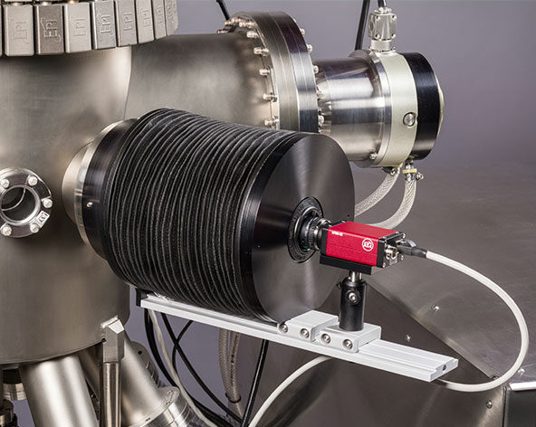
The kSA 400 analytical Reflection High-Energy Electron Diffraction (RHEED) system puts the power of RHEED at your fingertips. Whether analyzing a static diffraction pattern or acquiring data at multiple azimuths during substrate rotation, the kSA 400 makes quantitative RHEED analysis easy. Exploit the power of RHEED with the kSA 400!
The kSA 400 combines a high-resolution, high-speed, and high-sensitivity camera with sophisticated RHEED-specific acquisition and analysis software. This flexible system enables the analysis of virtually any image feature and, with one of many additional options, controls the electron gun for such tasks as acquiring RHEED rocking curves.
Easy to use and straightforward to install, the kSA 400 is designed for convenience and gives quantitative results right out of the box. Seamless integration between hardware and software as well as visually-driven RHEED pattern analysis, makes user operation straightforward and simple. Extensive customer input has helped us make the kSA 400 the industry’s most powerful analytical RHEED system and an integral part of MBE, PLD, PVD, and surface science chambers worldwide. Now in its fifth generation, the goal of the kSA 400 is to provide you with the most information from your RHEED pattern.
Growth Rate
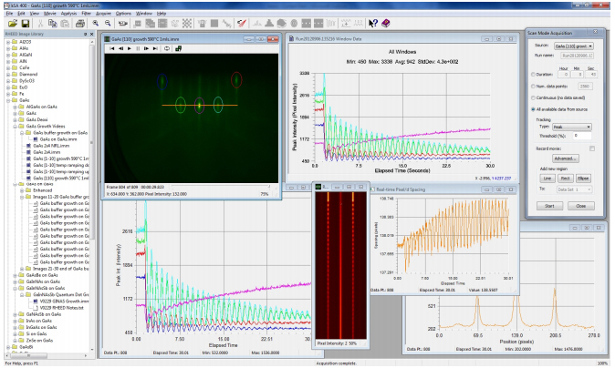
The most common use of RHEED is for determining growth rate via RHEED intensity oscillations, a phenomena that occurs during layer-by-layer epitaxial growth. The kSA 400 determines growth rate via three complimentary methods: Fourier-transform, extrema count (derivative analysis), and damped sine wave fitting. These three techniques determine growth rate independently, resulting in very accurate and consistent measurement of your thin-film growth rate. Watch the kSA 400 monitor RHEED oscillations. For more detailed information see our Growth Rate Methods application note
Lattice Spacing/Strain
Another powerful use for RHEED is to determine the absolute atomic spacing, or lattice spacing, between atoms on a surface. The kSA 400 makes measuring absolute lattice spacing simple. Furthermore, if you’d like to measure the evolution of lattice spacing, or the strain of lattice mismatched growth, the kSA 400 makes this easy too. By monitoring the spacing between diffraction streaks using sophisticated, proven analysis algorithms, strain evolution with very high accuracy and resolution is at your fingertips with the kSA 400.
Structural Analysis
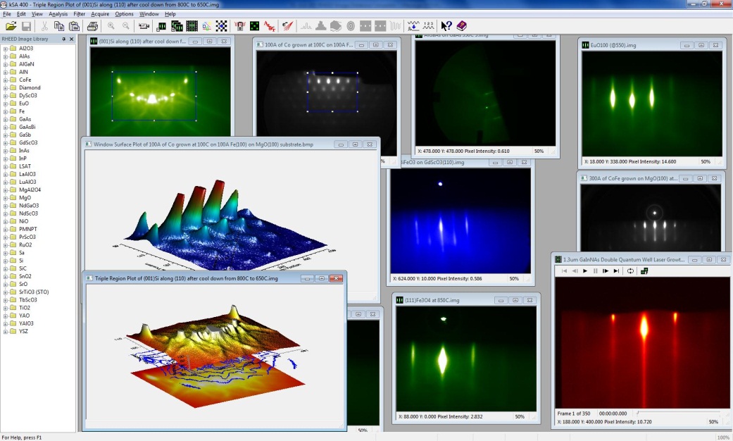
The kSA 400 makes analyzing surface structure easy. By acquiring RHEED images along the major crystal directions of the surface, measuring the pixel spacing and calculating a ratio, surface crystal structure can easily be determined. The kSA 400 also makes acquiring and archiving RHEED patterns a snap. The kSA 400 software contains a comprehensive RHEED Image Library (RIL) for reference and further analysis.
kSA 400
The kSA 400 is the most advanced, full featured RHEED data acquisition and analysis package available. With a long list of capabilities, and available plug-in options, the kSA 400 offers the most insight from RHEED patterns. The kSA 400 RHEED analysis software has camera control options; data acquisition modes; acquisition, image analysis, data analysis, and export capabilities; and data storage and communications options.
kSA 400 Lite
A RHEED acquisition and analysis package for those requiring only basic image capture and data analysis. The kSA 400 Lite package can be upgraded to the full featured version of kSA 400 at any time. The kSA 400 Lite RHEED analysis software has full camera control features; pared down data acquisition modes; acquisition, image analysis, data analysis, and export capabilities; and data storage and communications options.
kSA 400 AOS
An Analysis Only version designed for users who want to perform post-acquisition display, processing, and analysis away from the laboratory. The RHEED analysis-only software (kSA 400 AOS) license is available to users who currently own a full kSA 400 system.
What You Get With a kSA 400 System
- High resolution, high S/N camera
- Optic Mounts for mounting to the RHEED screen viewport
- Appropriate cabling
- kSA 400 or kSA 400 Lite software for the Win10 operating system
- kSA 400 RHEED Image Library (full version of kSA 400 only)
- Computer (optional)
The kSA 400 supports several plug-in options to give you even more analytical capability. These plug-ins include:
- Electron Gun Control
- LEED IV (Low Energy Electron Diffraction)
- PLE (Phase-Locked Epitaxy)
- Rotation Monitoring and Triggering
- Auger/XPS Acquisition
These options can be added to a standard kSA 400 system at any time, and typically include a software plug-in and hardware additions. One of our most popular plug-in options is RHEED Electron Gun Control, which allows you to control all the settings of your RHEED gun through the kSA 400 software. The kSA 400 software also allows you to acquire RHEED images while varying gun control parameters e.g. beam rocking acquisition which is supported on Staib beam rocking electron guns.

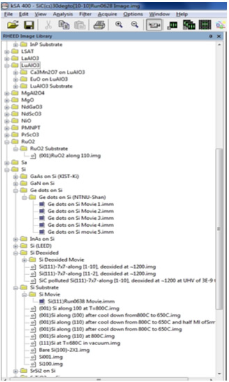
The kSA 400 RHEED Image Library (RIL) is a compilation of images and movies acquired from our kSA 400 customers, to the tune of ~ 30 gbytes of data. We have asked our customers to document the details of the conditions under which the data was taken, e.g. what the growth conditions are (temperature substrate, etc.), what the crystal orientation is, what the beam energy is, and so on. These details are either in the file name or in the Comments section of the file
We envision the use of the RIL to be mainly as a reference library for RHEED. Here are some examples of how we envision the RIL being used:
- You’re curious about what the oxide desorption process looks like for a GaAs substrate, so you load a GaAs desorb movie from the RIL and watch the evolution of the RHEED pattern as the oxide desorption occurs.
- You are working with SrTiO3 substrates, and you’d like to compare your RHEED patterns to those other researchers in your field are checking, for example, the width and length of the diffraction streaks as an indication of surface quality.
- You are teaching a surface science class and are on the topic of RHEED, and you’d like the students to check the ratio of lattice spacings along different crystal directions to verify the bcc structure of a material. You have the students pull up a GaAs movie, identify the major pull crystal directions (rotating substrate movie), and have them check the ratios of pixel spacings.
- You’d like to see what the growth of Ge quantum dots on Si looks like via RHEED.
- You’d like to look at GaAs on GaAs RHEED oscillations, and test our growth rate algorithms (we have 3 different algorithms in the kSA 400) on this movie data.

References
View All ReferencesTwo-dimensional Ferromagnetism in Eu-intercalated Few-layer Graphene
Ivan S. Sokolov, Dmitry V. Averyanov, Oleg E. Parfenov, Alexander N. Taldenkov, Igor A. Karateev, Andrey M. Tokmachev, Vyacheslav G. Storchak
Nanoscale Synthesis of Ionic Analogues of Bilayer Silicene with High Carrier Mobility
Dmitry V. Averyanov, Peitao Liu, Ivan S. Sokolov, Oleg E. Parfenov, Igor A. Karateev, Domenico Di Sante, Cesare Franchini, Andrey M. Tokmachev, and Vyacheslav G. Storchak
Carbonate Formation Lowers the Electrocatalytica Activity of Perovskite Oxides for Water Electrolysis
Christoph Baeumer, Allen Yu-Lun Liang, Urˇska Trstenjak, Qiyang Lu, Rainer Waser, J. Tyler Mefford, Felix Gunkel, Slavomir Nemsak, and William C. Chueh
The Role of Buffer Layer on the Performance and Uniformity Improvement of Long-Length HTS YBa2Cu3O7−x Tapes Derived by MOD
Chen Liao, Chuanbing Cai, Feng Fan, Yangyang Chen, Zhiyong Liu, Chuanyi Bai, Yuming Lu, Yanqun Guo, Hongbin Jian, and Yongjun Zhang
Emerging 2D Magnetic States in Graphene-based Monolayer of EuC6
Ivan S. Sokolov, Dmitry V. Averyanov, Fabrice Wilhelm, Andrei Rogalev, Oleg E. Parfenov, Alexander N. Taldenkov, Igor A. Karateev, Andrey M. Tokmachev, and Vyacheslav G. Storchak
Inhomogeneity Mediated Systematic Reduction of Schottky Barrier in Au/’GaN-nanorods-film’ Interface
Rohit Kumar Pant, Basanta Roul, Deependra Kumar Singh, Arun Malla Chowdhury, Karuna K. Nanda, and S B Krupanidhi
Thickness-driven Quantum Anomalous Hall Phase Transition in Magnetic Topological Insulator Thin Films
Yuchen Ji, Zheng Liu, Peng Zhang, Lun Li, Shifei Qi, Peng Chen, Yong Zhang, Qi Yao, Zhongkai Liu, Kang L. Wang, Zhenhua Qiao, and Xufeng Kou
Making BaZrS3 Chalcogenide Perovskite Thin Films by Molecular Beam Epitaxy
Ida Sadeghi, Kevin Ye, Michael Xu, James M. LeBeau, R. Jaramillo
Turning Electrochemically Driven Surface Transformation in Atomically Flat LaNiO3 Thin Films for Enhanced Water Electrolysis
Christoph Baeumer, Jiang Li, Qiyang Lu, Allen Yu-Lun Liang, Lei Jin, Henrique Perin Martins, Tomáš Duchoň, Maria Glöß Sabrina M. Gericke, Marcus A. Wohlgemuth, Margret Giesen, Emily E. Penn, Regina Dittmann, Felix Gunkel, Rainer Waser, Michal Bajdich, Slavomír Nemšák, J. Tyler Mefford and William C. Chueh
a-axis YBa2Cu3O7−x/PrBa2Cu3O7−x/YBa2Cu3O7−x Trilayers with Subnanometer RMS Roughness
Y. Eren Suyolcu, Jiaxin Sun, Berit H. Goodge, Jisung Park, Jürgen Schubert, Lena F. Kourkoutis, and Darrell G. Schlom
Mg3N2 Nanocrystallites Formation During the GaN:Mg Layers Growth by the NH3-MBE Technique
T.V. Malin, V.G. Mansurov, Yu.G. Galitsyn, D.S. Milakhin, D.Yu. Protasov, B.Ya. Ber, D. Yu. Kazantsev, V.V. Ratnikov, M.P. Shcheglov, A.N. Smirnov, V.Yu. Davydov, K. S. Zhuravlev
Formation of Quasi-Free-Standing Graphene on SiC(0001) Through Intercalation of Erbium
P. D. Bentley, T. W. Bird, A. P. J. Graham, O. Fossberg, S. P. Tear, and A. Pratt
Electo-optic Response in Epitaxially Stabilized Orthorhombic mm2 BaTiO3
Marc Reynaud, Pei-Yu Chen, Wente Li, Therese Paoletta, Sunah Kwon, Dae Hun Lee, Ilya Beskin, Agham B. Posadas, Moon J. Kim, Chad M. Landis, Keji Lai, John G. Ekerdt, and Alexander A. Demkov
Polarity-tunable Anomalous Hall Effect in Magnetic Topological Insulator MnBi2Te4
Lixuan Tai, Su Kong Chong, Huairuo Zhang, Peng Zhang, Peng Deng, Christopher Eckberg, Gang Qiu, Bingqian Dai, Haoran He, Di Wu, Shijie Xu, Albert V. Davydov, and Kang L. Wang
Influence of Composition and Morphology on the Electronic Properties of Semiconductor Nanostructures and Alloys
Christian M. Greenhill
Analysis of the AlN Phase Transition on a Sapphire Surface Within a Universal 2D Lattice Gas Model in MBE
D S Milakhin, T V Malin, V G Mansurov, Yu G Galitsyn and K S Zhuravlev
Classification of In Situ Reflection High Energy Electron Diffraction Images by Principal Component Analysis
Jinkwan Kwoen and Yasuhiko Arakawa
Growth Mode and Strain Effect on Relaxor Ferroelectric Domains in Epitaxial 0.67Pb(Mg1/3NB2/3)O3-0.33PbTiO3/SrRuO3 Heterosctructures
Jamal Belhadi, Urska Gabo, Hana Ursic, Nina Daneu, Jieun Kim, Zishen Tian, Gertjan Koster, Lane W. Martin, and Matjaz Spreitzer
Dimensional Stacking for Machine Learning in ToF‐SIMS Analysis of Heterostructures
Kevin Abbasi Hugh Smith Matthew Hoffman Elahe Farghadany Laura S. Bruckman Alp Sehirlioglu
Polarization Dependent Photoluminescence and Optical Anisotropy in CuPtB-Ordered Dilute GaAs1-XBix Alloys
Tadas Paulauskas, Bronislovas Čechavičius, Vytautas Karpus, Lukas Jočionis, Saulius Tumėnas, Jan Devenson, Vaidas Pačebutas, Sandra Stanionytė, Viktorija Strazdienė, Andrejus Geižutis, Mária Čaplovičová, Viliam Vretenár, Michael Walls, and Arūnas Krotkus
Comprehensive Analysis of Metal Modulated Epitaxial GaN
Habib Ahmad, Keisuke Motoki, Evan A. Clinton, Christopher M. Matthews, Zachary Engel, and W. Alan Doolittle
Dimensionality Concept in Solid-State Reactions: A Way to Control Synthesis of Functional Materials at the Nanoscale
Andrey M. Tokmachev, Dmitry V. Averyanov, Igor A. Karateev, Ivan S. Sokolov, Oleg E. Parfenov, Vyacheslav G. Storchak
Band Gap Engineering Studies of PbTe, StTe, and CdSeTe for CDTE Solar Cell Applications
Elizabeth G. LeBlanc
Combined In Situ XRD and Ex Situ TEM Studies of Thin Ba0.5Sr0.5TiO3 Films Grown by PLD on MgO
Sondes Bauer,* Adriana Rodrigues, Xiaowei Jin, Reinhard Schneider, Erich Müller, Dagmar Gerthsen, and Tilo Baumbach
Classification of Reflection High-Energy Electron Diffraction Pattern Using Machine Learning
Jinkwan Kwoen and Yasuhiko Arakawa
Spontaneous Positive Exchange Bias Effect in SrFeO3-x/SrCoO3-x Epitaxial Bilayer
Tian-Cong Su, Jun Zhang, Wei Zhang, Ying-Ying Wang, Hui-Hui Ji, Xiao-Jiao Wang, Guo-Wei Zhou, Zhi-Yong Quan & Xiao-Hong Xu
Large Exchange Splitting in Monolayer Graphene Magnetized by an Antiferromagnet
Yingying Wu, Gen Yin, Lei Pan, Alexander J. Grutter, Quanjun Pan, Albert Lee, Dustin A. Gilbert, Julie A. Borchers, William Ratcliff II, Ang Li, Xiao-dong Han & Kang L. Wang
Giant Quadratic Magneto-Optical Kerr Effect in (Eu,Gd)O Films for Magnetic Field Sensing
Vladimir N. Kats, Sergey G. Nefedov, Leonid A. Shelukhin, Pavel A. Usachev, Dmitry V. Averyanov, Igor A. Karateev, Oleg E. Parfenov, Alexander N. Taldenkov, Andrey M. Tokmachev, Vyacheslav G. Storchak, Victor V. Pavlova
Beam Rocking Auger Electron Spectroscopy of a Si(111)√3×√3-Ag Surface
Yoshimi Horio, Hitoshi Nakahara, Junji Yuhara, Yuji Takakuwa
Roles of Strain and Carrier in Silicon Oxidation
Shuichi Ogawa, Akitaka Yoshigoe, Jiayi Tang, Yuki Sekihata, and Yuji Takakuwa
Machine Learning Analysis of Perovskite Oxides Grown by Molecular Beam Epitaxy
Sydney R. Provence, Suresh Thapa, Rajendra Paudel, Tristan Truttmann, Abhinav Prakash, Bharat Jalan, Ryan B. Comes
Highly Responsive, Self-Powered a-GaN Based UV-A Photodetectors Driven by Unintentional Asymmetrical Electrodes
Rohit Pant, Deependra Kumar Singh, Arun Mall Chowdhury, Basanta Roul, Karuna Kar Nanda, and Saluru Baba Krupanidhi
Stabilization of the Perovskite Phase in PMN-PT Epitaxial Thinfilms via Increased Interface Roughness
Urška Gabor, Damjan Vengust, Zoran Samardžija, Aleksander Matavž, Vid Bobnar, Danilo Suvorov, MatjažSpreitzer
Physicochemical Aspects of the Formation of AlN Crystal Film on the (0001)Al2O3 Surface
V.G. Mansurov, Yu. G. Galitsyn, Yu. I. Mikhailov, T.V. Malin, D.S. Milakhin, K.S. Zhuravlev
Layer-Controlled Laws of Electron Transport in Two-Dimensional Ferromagnets
Oleg E. Parfenov, Andrey M. Tokmachev, Dmitry V. Averyanov, Igor A. Karateev, Ivan S.Sokolov, Alexander N. Taldenkov, Vyacheslav G. Storchak
Epitaxial n++-InGaAs Ultra-Shallow Junctions for Highly Scaled n-MOS Devices
P. Tejedor, M. Drescher, L. Vázqueza, L. Wildeb
Probing Proximity Effects in the Ferromagnetic Semiconductor EuO
Dmitry V. Averyanov, Andrey M.Tokmachev, Oleg E.Parfenov, Igor A.Karateev, Ivan S.Sokolov, Alexander N.Taldenkov, Mikhail S.Platunov, Fabrice Wilhelm, AndreiRogalev, Vyacheslav G.Storchak
Investigation into the Memristor Effect in Nanocrystalline ZnO Films
Smirnov, V.A., Tominov, R.V., Avilov, V.I. et al.
Photodetection Properties of Nonpolar a‐Plane GaN Grown by Three Approaches Using Plasma‐Assisted Molecular Beam Epitaxy
Rohit Kumar Pant Deependra Kumar Singh Basanta Roul Arun Malla Chowdhury Greeshma Chandan Karuna K. Nanda Saluru B. Krupanidhi
Electron-Stimulated Aluminum Nitride Crystalline Phase Formation on the Sapphire Surface
Denis Milakhin, Timur Malin, Vladimir Mansurov, Yury Galitsyn, Konstantin Zhuravlev
Real-time monitoring and control of nitride growth rates by Metal Modulated Epitaxy
Kent L. Averett, John B. Hatch, Kurt G. Eyink, Cynthia T. Bowers, Krishnamurthy Mahalingam
Interface-Induced Anomalous Hall Conductivity in a Confined Metal
Oleg E. Parfenov, Dmitry V. Averyanov, Andrey M. Tokmachev, Igor A. Karateev, Alexander N. Taldenkov, Oleg A. Kondratev, and Vyacheslav G. Storchak
High Mobility Single-Crystalline-Like Silicon Thin Films on Inexpensive Flexible Metal Foils by Plasma Enhanced Chemical Vapor Deposition
P.Dutta, Y.Gao, M. Rathi, Y. Yao, Y.Li, M. Iliev, J. Martinez, V. Selvamanickam
Order Parameter and Band Gap of ZnSnN2
R. A. Makin et al.
Atomic Structure of Sr/Si(001)(1×2) Surfaces Prepared by Pulsed Laser Deposition
Tjaša Parkelj Potočnik, Erik Zupanič, Wen-Yi Tong, Eric Bousquet, Daniel Diaz Fernandez, Gertjan Koster, Philippe Ghosez, Matjaž Spreitzer
Stress Generation and Evolution in Oxide Heteroepitaxy
Aline Fluri, Daniele Pergolesi, Alexander Wokaun, and Thomas Lippert
An Experimental Study of Residual Stress Induced Modulation of Vibration Characteristics in 1-D MEMS Resonators
Behera, A., Dangi, A., and Pratap, R.
Emerging Two-Dimensional Ferromagnetism in Silicene Materials
Andrey M. Tokmachev, Dmitry V. Averyanov, Oleg E. Parfenov, Alexander N. Taldenkov, Igor A. Karateev, Ivan S. Sokolov, Oleg A. Kondratev & Vyacheslav G. Storchak
Role of the Phase Transition at GaN QDs Formation on (0001)AlN Surface by Ammonia Molecular Beam Epitaxy
Konfederatova, K.A., Mansurov, V.G., Malin, T.V. et al.
Room-Temperature Growth of Thin Films of Niobium on Strontium Titanate (0 0 1) Single-Crystal Substrates for Superconducting Joints
Yuhei Shimizu, Kazuhiko Tonooka, Yoshiyuki Yoshida, Mitsuho Furuse, Hiroshi Takashima
Direct epitaxial integration of the ferromagnetic semiconductor EuO with Si(1 1 1)
Dmitry V. Averyanov, Peter E. Terin, Yuri G. Sadofyev, Andrey M. Tokmachev, Alexey E. Primenko, Igor A. Likhachev & Vyacheslav G. Storchak
Preparation of YBa2Cu3O7−δ and La1.85Sr0.15CuO4 Bilayer Structure for Superconducting Connection
Yuhei Shimizu , Hiroshi Takashima, Yoshiyuki Yoshida, and Mitsuho Furuse
Emerging Two-Dimensional Ferromagnetism in Silicene Materials
Andrey M. Tokmachev1, Dmitry V. Averyanov1, Oleg E. Parfenov1, Alexander N. Taldenkov1, Igor A. Karateev1, Ivan S. Sokolov1, Oleg A. Kondratev1 & Vyacheslav G. Storchak
Influence of Surface Structures on Quality of CdTe (100) Thin Films Grown on GaAs (100) Substrates
Yi Gu, Hui-Jun Zheng, Xi-Ren Chen, Jia-Ming Li, Tian-Xiao Nie, Xu-Feng Kou
Control of Spin-Wave Damping in Radio Frequency Components Using Spin Currents from Topological Insulators
A Navabi-Shirazi
High-Temperature Magnetism in Graphene Induced by Proximity to EuO
Dmitry V. Averyanov, Ivan S. Sokolov, Andrey M. Tokmachev, Oleg E. Parfenov, Igor A. Karateev, Alexander N. Taldenkov, and Vyacheslav G. Storchak
Role of the Phase Transition at GaN QDs Formation on (0001) AlN Surface by Ammonia Molecular Beam Epitaxy
Kseniya A. Konfederatova, Vladimir G. Mansurov, Timur V. Malin, Yurij G. Galitsyn, Ivan A. Aleksandrov, Vladimir I. Vdovin, Konstantin S. Zhuravlev
Indium Thin Films in Multilayer Superconducting Quantum Circuits
McRae, Corey Rae
Coupling of Magnetic Orders in a 4f Metal/Oxide System
Dmitry V. Averyanov, Andrey M. Tokmachev, Oleg E. Parfenov, Igor A. Karateev, Alexander N. Taldenkov and Vyacheslav G. Storchak
Growth of Ordered and Disordered ZnSnN2
Robert Allen Makin, Nancy Senabulya, James Mathis, N. Feldberg, P. Miska, Roy Clarke, and Steven M. Durbin
High Mobility Single-Crystalline-Like Silicon Thin Films on Inexpensive Flexible Metal Foils by Plasma Enhanced Chemical Vapor Deposition
P.Dutta, Y.Gao, M.Rathi, Y.Yao, Y.Li, M.Iliev, J.Martinez, V.Selvamanickama
Thin Film Metrology and Microwave Loss Characterization of Indium and Aluminum/Indium Superconducting Planar Resonators
C.R.H. McRae, J.H. Béjanin, C.T. Earnest, T.G. McConkey, J.R. Rinehart, C. Deimert, J.P. Thomas, Z.R. Wasilewski, and M. Mariantoni
Anisotropic Magnetic Damping Studies in β-Ta/2D-Epitaxial-Py Bilayers
Nilamani Behera, Ankit Kumara, Dinesh K.Pandya, SujeetChaudhary
Photo- and Cathodoluminescence of Eu3+ or Tb3+ Doped CaZrO3 Films Prepared by Pulsed Laser Deposition
Kazushige Ueda, Yuhei Shimizu, Hiroshi Takashima, Florian Massuyeau, Stéphane Jobic
Interfacial Misfit Array Technique for GaSb Growth on GaAs(001) Substrate by Molecular Beam Epitaxy
D. Benyahia, Ł. Kubiszyn, K. Michalczewski, A. Keblowski, P. Martyniuk, J. Piotrowski, and A. Rogalski
Engineering of Magnetically Intercalated Silicene Compound: An Overlooked Polymorph of EuSi2
Andrey M. Tokmachev, Dmitry V. Averyanov, Igor A. Karateev, Oleg E. Parfenov, Oleg A. Kondratev, Alexander N. Taldenkov, Vyacheslav G. Storchak
Epitaxial stabilization of ordered Pd–Fe structures on perovskite substrates
Renee M. Harton, Vladimir A.Stoica, RoyClarke
Tin Oxide Films Grown by Molecular Beam Epitaxy
Gazoni, Martinez
The Interplay of Surface Adsorbates and Cationic Intermixing in the 2D Electron Gas Properties of LAO-STO Heterointerfaces
Akrobetu, Richard K
Structural Characterization Studies on Semiconducting ZnSnN2 Films using Synchrotron X-ray Diffraction
Senabulya, Nancy
Chapter Nine – Dynamic Atomic Layer Epitaxy of InN on/in GaN and Its Application for Fabricating Ordered Alloys in Whole III-N System
K. Kusakabe, A. Yoshikawa
Two Magnon Scattering and Anti-Damping Behavior in a Two-Dimensional Epitaxial TiN/Py(tPy)/b-Ta(tTa) System
Nilamani Behera, Ankit Kumar, Sujeet Chaudhary and Dinesh K. Pandya
A Prospective Submonolayer Template Structure for Integration of Functional Oxides with Silicon
Dmitry V. Averyanov, Christina G. Karateeva, Igor A. Karateev, Andrey M. Tokmachev, Mikhail V. Kuzmin, Pekka Laukkanen , Alexander L. Vasiliev, Vyacheslav G. Storchak
In Situ Stress Observation in Oxide Films and How Tensile Stress Influences Oxygen Ion Conduction
Aline Fluri, Daniele Pergolesi, Vladimir Roddatis, Alexander Wokaun and Thomas Lippert
Topotactic Synthesis of the Overlooked Multilayer Silicene Intercalation Compound SrSi 2
Andrey Tokmachev, Dmitry Averyanov, Igor Karateev, Oleg Parfenov, Alexander L. Vasiliev, Sergey Yakunin and Vyacheslav Storchak
Atomic-Scale Engineering of Abrupt Interface for Direct Spin Contact of Ferromagnetic Semiconductor with Silicon
Dmitry V. Averyanov, Christina G. Karateeva, Igor A. Karateev, Andrey M. Tokmachev, Alexander L. Vasiliev, Sergey I. Zolotarev, Igor A. Likhachev & Vyacheslav G. Storchak
Disentanglement of Growth Dynamic and Thermodynamic Effects in LaAlO3/SrTiO3 Heterostructures
Chencheng Xu, Christoph Bäumer, Ronja Anika Heinen, Susanne Hoffmann-Eifert, Felix Gunkel & Regina Dittmann
Nanocrystalline Ferroelectric BiFeO3 Thin Films by Low Temperature Atomic Layer Deposition
Mariona Coll, Jaume Gazquez, Ignasi Fina, Zakariaya Khayat, Andy Quindeau, Marin Alexe, Maria Varela, Susan Trolier-McKinstry , Xavier Obradors, and Teresa Puig
Observation of Inverse Spin Hall Effect in Bismuth Selenide
Praveen Deorani, Jaesung Son, Karan Banerjee, Nikesh Koirala, Matthew Brahlek, Seongshik Oh, and Hyunsoo Yang
Review on RHEED – Reflective High Energy Electron Diffraction (RHEED)- A Unique Tool For In-Situ Growth Monitoring
Oleg Maksimov, Material Research Institute, Pennsylvania State University
In Situ Composition Monitoring Using RHEED for SrTiO3 Thin Films Grown by Reactive Coevaporation
Luke S.-J Peng and Brian H. Moeckly
Smoothening of Cu Films Grown on Si(001)
R. A. Lukaszew, Y. Sheng, C. Uher, and R. Clarke
RHEED Monitoring of Rotating Samples During Large-Area Homogeneous Deposition of Oxides
V. C. Matijasevic, Z. Lu, K. Von Dessonneck, C. Taylor, D. Barlett
Growth and Magnetic Properties of Co x Ni 1-x Ultrathin Films on Cu(100)
F. O. Schumann, S. Z. Wu, G. J. Mankey, and R. F. Willis
Temperature-Dependent Strain Relaxation and Islanding of Ge/Si(111)
P. W. Deelman, L. J. Schowalter, and T. Thundat
Resonant RHEED Study of Cu 3Au(111) Surface Order
S. W. Bonham and C. P. Flynn
Molecular Beam Epitaxial Growth of InAs/AlGaAsSb Deep Quantum Wells on GaAs Substrates
N. Kuze, H. Goto, S. Miya, S. Muramatsu, M. Matsui, I. Shibasaki
Studies of Exchange Coupling in Fe(001) Whisker/Cr/Fe Structures Using BLS and RHEED Techniques
B. Heinrich, M. From, J. F. Cochran, L. X. Liao, Z. Celinski, C. M. Schneider and K. Myrtle
The Use of RHEED Intensities for the Quantitative Characterization of Surfaces
Y. Ma, S. Lordi and J. A. Eades
Morphology Transition and Layer-by-Layer Growth of Rh(111)
F. Tsui, J. Wellman, C. Uher, and Roy Clarke
Review on RHEED – Introduction to RHEED
A.S. Arrot
Structural transition in epitaxial Co-Cr superlattices
W. Vavra, D. Barlett, S. Elagoz, C. Uher, and R. Clarke
camera-Based RHEED Detection and Analysis System
D. Barlett, C.W. Snyder, B.G. Orr, and Roy Clarke
The Molecular Beam Epitaxy Growth of InGaAs on GaAs(100) Studied by In Situ Scanning Tunneling Microscopy and Reflection High-Energy Electron Diffraction
C. W. Snyder, D. Barlett, B. G. Orr, P. K. Bhattacharya and J. Singh
Review on RHEED – A Review of the Geometrical Fundamentals of RHEED with Application to Silicon Surfaces
John E. Mahan, Kent M. Geib, G.Y. Robinson, and Robert G. Long