
Application Notes : kSA MOS – Resolution and Sensitivity
Version: 1.0
Resolution and sensitivity of stress measurements with the
k-Space Multi-beam Optical Sensor (MOS) System
by Eric Chason
for k-Space Associates
A wide variety of technologies rely on thin films. In microelectronics, magnetic storage and optical communications (to name a few), thin films are critical to obtaining high performance and reliability. In many of these applications, residual stress in the thin films can severely limit their capabilities or lifetime.
In order to understand how to control this important parameter, the first step is to quantify the film stress and stress evolution. To measure stress in thin films, we have developed the k-Space MOS (Multi-beam Optical Sensor) System. MOS is a non-destructive optical technique that measures the curvature induced in the sample by stress in the thin film. It can be used for ex sit u characterization or in sit u real-time monitoring of stress evolution.
The purpose of this application note is to discuss the measurement issues that determine both the resolution and the sensitivity of the MOS technique. Determining the resolution means understanding the sources of error on the measured value of the stress or curvature. Because the MOS system has capabilities for both static and dynamic stress measurements, we discuss the different resolution for absolute stress values and relative changes in the stress. Determining the sensitivity is equivalent to evaluating the minimum stress that can be measured. Sensitivity is influenced by a number of thin film and measurement para meters, so the dependence on substrate, thin film and measurement conditions is also discussed.
The results discussed in this application note correspond to scenarios and experimental configurations that can be achieved fairly routinely. With care to reduce sources of noise, higher sensitivities and resolution have been obtained. The results discussed here should be taken more as guidelines than as absolute limits. In the following sections, we first discuss the principle behind the MOS measurement. This is followed by a discussion of the resolution of the technique and the sensitivity.
Optical Stress Measurement Technique
In order to understand the limits on resolution of the MOS system (or any curvature based stress measurement), it is necessary to understand the principle behind the measurement. As originally described by Stoney, stress in a thin film induces curvature in the substrate. The change in curvature  is related to the film stress
  by the well-known Stoney equation:
![\[ \kappa-\kappa_0 = \frac{6\sigma h_f}{M_sh_s^2} \quad \quad \quad(1) \]](https://k-space.com/wp-content/ql-cache/quicklatex.com-871b00df6b6b34d444a8ee67a2a31774_l3.png "Rendered by QuickLaTeX.com")
 is the initial curvature of the unstressed substrate. The other parameters in this equation are the film thickness (
 ), biaxial modulus of the substrate (
 ) and the substrate thickness (
 ). The radius of curvature,
  , is equal to
  . The biaxial modulus of the film is related to the bulk modulus (
 ) by the Poisson ration (
 ):
):
![\[M_s = \frac{E}{1-v} \quad \quad \quad (2) \]](https://k-space.com/wp-content/ql-cache/quicklatex.com-862a3e74aca5c8b3acda617925078e6b_l3.png "Rendered by QuickLaTeX.com")
The key to this type of stress measurement is therefore obtaining a precise measurement of the curvature. A schematic of the MOS apparatus for measuring sample curvature optically is shown in figure 1. In the MOS approach, the sample is illuminated by an array of parallel laser beams. The actual measurement consists of determining the spacing of the beams reflected from the surface when they arrive at the face of the CCD camera. If the surface is flat, the beams will have the same spacing after being reflected as they had in the incident beam array. If the surface is curved, the beams will be deflected and the spacing of the beams on the CCD will be change. The change in the spacing of the reflected beams due to stress-induced curvature is monitored on a CCD camera.
The spacing between the beams is a direct measure of the substrate curvature. As shown in figure 2, the curvature change induced by the stress is related to the measured deflection of the beams by:
![\[ \kappa - \kappa_0 = \left ( \frac{\delta d}{d_0} \right ) \frac{cos \alpha }{2L} \quad \quad \quad (3) \]](https://k-space.com/wp-content/ql-cache/quicklatex.com-e36718bfd86e41b8afee60f98e6ac307_l3.png "Rendered by QuickLaTeX.com")
 is the difference in beam spacing from the initial spacing,
  , due to the stress-induced curvature. The ratio
  is referred to as the differential spacing. The distance of the sample from the camera is
  and the angle between the beam array and the sample normal is
  . Combining this measurement with the Stoney formula shows that the measured stress is directly proportional to the measured deflections of the beams, as given by:
![\[ \sigma h_f = \left ( \frac{\delta d}{d_0} \right ) \frac{M_s h_s^2 \cos \alpha}{12L} \quad \quad \quad (4) \]](https://k-space.com/wp-content/ql-cache/quicklatex.com-4d9cd6e6d68d888794148ff64f56fef8_l3.png "Rendered by QuickLaTeX.com")
Resolution
From the equations above, the measurement of stress corresponds to measuring the change in spacing of the reflected beams incurred by stress in the film. There are two dominant sources of error in this measurement. The first is the noise or error in the measurement of the beam spacing from a single sample. The second is determining the difference in the beam spacing that is due to stress in the film. These two aspects of the resolution are considered below.
1) Resolution in the measurement of beam spacing
When measuring the spacing between the beams, there is an error or noise in the measured value even when the sample is not changing. This noise may have many possible sources (drift in the detector, variation of the light source, thermal drift, etc.) but it’s not necessary to know the source to evaluate it. We define the stability of the system as the standard deviation of the measured beam spacing when the measurement configuration and sample are not intentionally changed. The stability is one of the major factors in determining the stress resolution. For example, suppose the MOS system is used to measure the change in stress during annealing of a film for one hour. To determine the error bars associated with this measurement, we need to know how much the measured beam spacing would be expected to vary over this time period if the sample were left completely unchanged. We want the measured change to be larger than the noise for the result to be significant.
An example of the stability of a table-top MOS setup is shown in figure 3. The data corresponds to the measurement of the spacing of beams reflected from a flat dielectric mirror over a period of 3000 s. The average value of the spacing is 379.88 pixels and the standard deviation of the measurement is 0.155 pixels or 0.04% of the measured spacing. Note that the data are randomly distributed around the average value, indicating that there is no significant systematic drift in the signal.
The measured standard deviation corresponds to the error that can be expected from a single measurement of the beam spacing. Since the data acquisition rate is rapid (approximately 0.1 second per data point), multiple measurements can be acquired so that the signal can be averaged over multiple measurements. In general, by averaging N points we reduce the noise by a factor of √N. So averaging 25 points, for instance, reduces the error on the average value of the beam spacing to 0.031 pixels or 0.008% of the measured beam spacing. If the camera is spaced 1 m from the sample (a typical value), this corresponds to a minimum resolvable curvature of 4 x 10⁻⁵ m-1 or a maximum radius of curvature of 25 kM. In the configuration used for these measurements, the sample was stably mounted so that vibration was minimal (the effect of sample vibration during in situ measurements is discussed below). For measurements where an even higher sensitivity is needed, special care must be used to reduce noise in the CCD, stray light, vibration, etc. When noise is reduced, maximum radii of curvature greater than 50 kM have been achieved.
2) Resolution in the measurement of changes due to stress
As discussed above, the stress is proportional to δd/d0where δd is the change in the beam spacing due to stress-induced curvature and d0 is the initial spacing of the MOS beams. In order to determine δd, we need to know the spacing of the beams from the sample before the stressed film has been put on it and after the stressed film has been added. There are two different approaches to obtaining this value, depending on whether the change in the curvature is measured in situ during processing or measured ex situ before and after a film is applied. In the case of in situ monitoring, we can directly measure the evolution of curvature as the film stress changes, while in the ex situ case we use a reference standard to compare absolute measurements of the curvature. The different resolutions associated with these approaches is discussed below.
In situ or relative measurements: This approach is used when the sample curvature can be monitored in situ during processing to monitor the change in the curvature as the stressed film is added to the substrate. The capability for in situ measurements is one of the primary advantages of MOS measurements. Other techniques are not easily adapted to measurement during processing or deposition. In the case of in situ measurements, it is not necessary to know the absolute curvature of the sample. A series of measurements of the beam spacing are made before the processing is started and this spacing is used as a baseline. After the processing starts, the change in the beam spacing is monitored continuously.
An example of data taken this way is shown in figure 4 which corresponds to deposition of an epitaxial layer of InxGa1-xAs on a aGaAs (001) substrate. The measurements are made in an MBE system at a temperature of 469°C. From time t=0 to 50s, the sample is measured at the constant growth temperature but the growth shutters are closed and no film is deposited. At time t=50s, the growth shutter is opened and a film is deposited at a constant growth rate of 0.23nm/s. After growth starts, the beam spacing is observed to increase linearly with the increasing time.
The change in curvature due to the deposited film is calculated from the measured change in the beam spacing. The initial spacing, d0, is determined by averaging the 200 measurements made between t=0s and t=50s. The change in spacing, δd, is the difference between the measured spacing after growth and d0. These values can then be used in equations 3 and 4 to calculate the curvature change and the product of stress and thickness in the deposited film. Note that in obtaining the stress, we do not need to know the absolute curvature of the sample. It is sufficient just to measure the change in beam spacing as the film was growing. From the known constant growth rate, we can easily convert the growth time to film thickness. The linear increase in the beam spacing with time (or thickness), indicates that the stress in the film is constant, i.e., no relaxation is taking place. The slope of the line in figure 4 is proportional to the stress in the film and the constants of proportionality are evaluated using equation 4. From the measured stress, we calculate the lattice mismatch between the film and the substrate and hence determine the film composition to be x=0.156. Subsequent X-ray measurements of the film composition indicate a value of x=0.165, in good agreement and within our measurement error of the substrate thickness.
To determine the resolution of the stress measurement, we must consider the error in the value of the original spacing, d0, and of the spacing after growth. The standard deviation of the spacing before growth starts is 0.62 pixels or 0.15% of the spacing. This measurement is some what noisier than the mirror measurement described above since this measurement was made in situ in the MBE chamber. Averaging the first 100 points, however, significantly reduces the noise. To look at the noise on the measurement after growth is started, we subtract a line corresponding to a fit to the data. The residual after the line is subtracted is shown in the inset in figure 4. The standard deviation of the residual is 0.68 pixels, only slightly larger than before growth is started. Because the MOS technique is sensitive to small beam spacing changes, it is therefore possible to measure small film stresses. The minimum stress that can be resolved based on this measurement resolution is discussed in the final section on sensitivity.
Absolute curvature measurements: This approach is typically used for ex situ measurements, where the change in the sample curvature during processing cannot be monitored continuously. The absolute curvature is measured before and after the film has been processed and the difference in the curvature is used to calculate the value of σhf. If the sample is not measured before deposition, we must assume that the surface was initially flat (κ0=0). This may limit the sensitivity of the measurement since even small amounts of figure error will lead to measurable differences in the curvature.
For these absolute measurements of curvature, a reference standard is used to determine the reference beam spacing, d0, corresponding to a flat surface. The difference of the beam spacing between the standard and the sample is used to calculate δd/d0 and obtain the curvature using equation (3). We typically use a dielectric coated mirror with a surface figure of λ/20 as our standard, so the error due to the curvature of the reference mirror is insignificant. The use of the standard has the effect of eliminating any error that may occur due to long term drifts in the system (or changes in the alignment by different operators).
Aside from long term drift in the measurement system, there are other potential sources of noise when the sample is removed between measurements. Non-uniformities in deposition or figure error in the starting surface may lead to a variation in curvature across the sample. Therefore, it is necessary to make sure that the sample is measured at the same position before and after the deposition of the film. The degree of this non-uniformity can be estimated by measuring the curvature at multiple places on the sample and the standard deviation in these measurements can be used to estimate the error on the actual curvature. Note that this source of error is not a problem for the relative measurements since the sample is always measured at the same position during processing.
Since the error due to sample in homogeneity depends on the sample, it is not possible to estimate its magnitude in general. A lower limit to the error can be obtained by looking at the deviation in measurements of the mirror over a number of samples. In figure 5 we show a measurement of the beam spacing obtained from the mirror after it was removed and replaced 25 times over a period of 6 hours. The standard deviation of the measurement is 0.22 pixels or 0.10% which is only a little larger than the error associated with system stability (0.155 pixels) shown in figure 3. Therefore, if the sample is uniform, we do not introduce a significant amount of error by remounting the standard and the sample.
3) The effect of sample vibration on resolution
The MOS technique was originally invented as a way of sensitively measuring stress in situ during deposition or other processing. In many processing chambers, there is a large ambient vibration noise due to equipment such as vacuum pumps. The parallel beam illumination was developed as a way to decrease the sensitivity to vibration. In optical techniques that use a single beam rastered across the surface, the measured position of the beam changes due to vibration of the sample and this noise can significantly decrease the resolution of the curvature measurement. By using parallel beam illumination, however, all the beams strike the surface at the same time. The beam spacing (i.e., the difference in the positions of adjacent beams that is used to calculate the curvature) is much less sensitive to the sample vibration than the absolute position of the beam.
The decrease in noise achieved by this approach is shown in figure 6. In the upper part of the figure, the position of one of the beams reflected from the surface is shown as a function of time. The sample is mounted on a manipulator in a vacuum chamber and the vibration leads to a large deviation of the beam position with time. The beam position has a standard deviation of 4.33 pixels. The beam spacing measured from the difference between two adjacent beam positions is shown in the lower part of the figure. The scale is identical to the one for the absolute beam position. The standard deviation of the measured spacing is only 0.09 pixels, a factor of 50 less than the noise on the absolute beam position. Since both beam positions are affected by vibration in essentially the same manner, the difference between them is relatively unaffected by the vibration.
Sensitivity
The above discussion concerned sources of error that limit our measurement of the curvature. In this section, we will discuss how the beam spacing resolution translates into limits on measurements of the stress. Because the curvature measures the product of stress and thickness, determination of the smallest stress that can be measured must be specified relative to the thickness of the film. A film with a stress of 1 GPa will induce 1000 times as much curvature for a film thickness of 1 micron than it will for a thickness of 1 nm. Furthermore, the ratio between the curvature and the stress depends on the square of the substrate thickness. So a film that induces a radius of curvature of 10 m on a substrate of 100 micron thickness will induce a 1 kM radius of curvature on a substrate of 1 mm thickness.
To calculate the stress sensitivity of MOS, we assume a resolution in the differential spacing (δd/d0) of 0.05%. The minimum resolvable stress is shown in figure 7 as a function of the film thickness. The data is plotted on a log scale to show the wide range of possible values that can be obtained. These calculations were made assuming that the modulus of the substrate is 100 GPa. The different colored lines on the graph correspond to different thicknesses of the substrate, from 100 microns to 1mm.
For a substrate of 100 microns, the measurement resolution makes the limit on the product of stress and thickness equal to 6×10⁻⁵ GPa -micron so that the minimum resolvable stress is given by (6×10⁻⁵/hf) GPa where hf is the film thickness in microns. This means that a film with 1 GPa stress can be measured for films with a thickness as low as 6×10⁻⁵ microns or equivalently 0.6 angstroms. This corresponds to less than a monolayer of Ge deposited on a Si surface, so that the effect of sub-monolayer coverages can even be determined. Much smaller stresses can be measured on thicker films. For a 1 micron metal film, for instance, a stress as low as 10-4 GPa (0.1 MPa) can be measured.
Figures
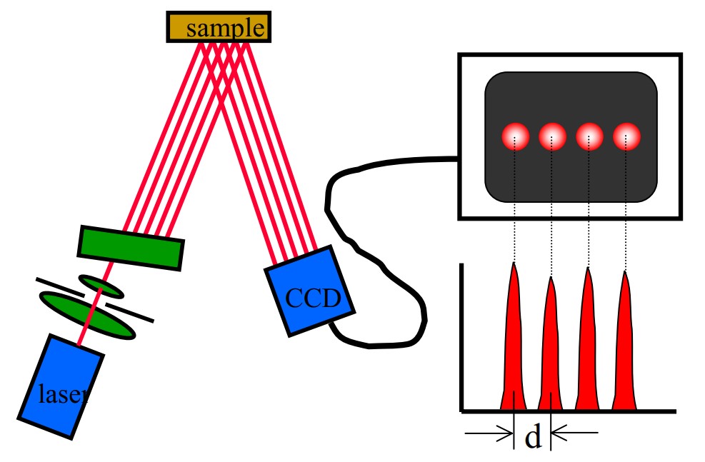
Figure 1: The MOS system uses an array of parallel beams to illuminate the sample. The position of the beams is measured with a CCD camera. A frame-grabber digitizes the image and the MOS software calculates the beam spacing, d. Stress-induced curvature in the sample changes the spacing of the reflected beams as shown in figure 2.

Figure 2: Stress in thin films induces curvature in the substrate. The MOS system measures the curvature optically by monitoring the deflection of parallel beams of light.
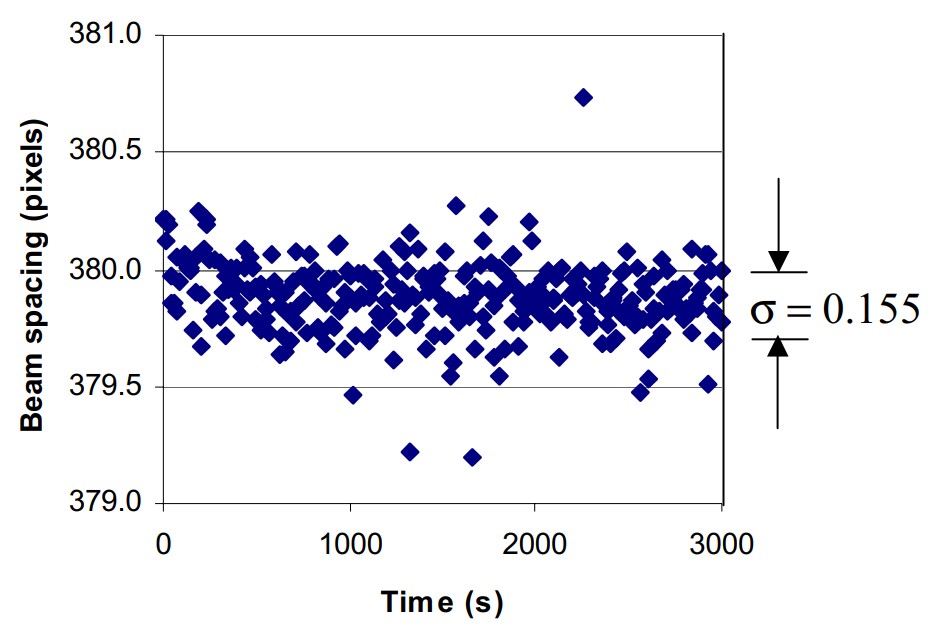
Figure 3: Stability of MOS measurement. The measurement shows the spacing of the beams reflected from a dielectric mirror in units of pixels on the CCD detector. The spacing was measured for 3000 s resulting in a standard deviation of 0.155 pixels.
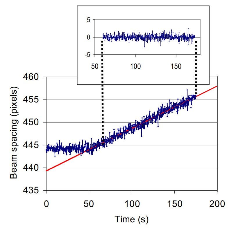
Figure 4: Beam spacing during epitaxial growth of InxGa1-xAs on GaAs(100). Growth is initiated at t=50 s at a rate of 0.23 nm/s. The red line corresponds to the best fit for growth of a film with constant stress. The difference between the measurement and the fit is shown in the inset.
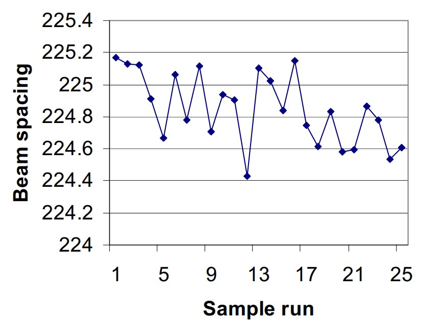
Figure 5: The beam spacing obtained from repeated measurements of a flat mirror over a 6 hr. period. The mirror was remounted before each measurement. The standard deviation of the measurement is 0.10%, similar to the stability of the system.
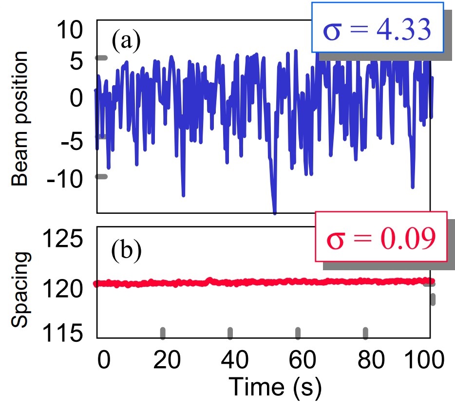
Figure 6: Reduction of noise during in situ curvature measurements by using multiple beams. a) Relative position of one of the MOS beams in units of pixels. The RMS deviation of 4.33 pixels is caused by sample vibration. b) Measurement of the spacing between adjacent MOS beams taken at same time as data in (a). The RMS deviation is 0.09, much lower than the single beam measurement.
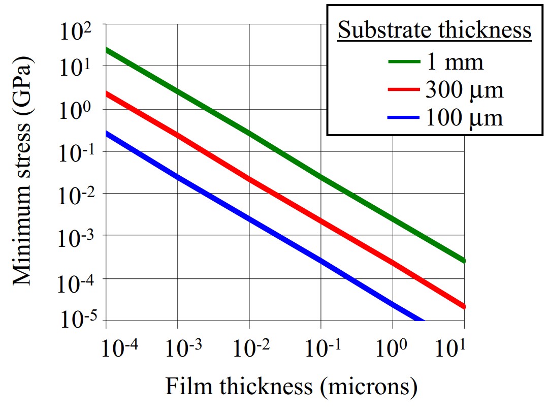
Figure 7: Sensitivity of MOS system for different film and substrate thicknesses. The modulus used for these calculations is 100 GPa and the minimum resolvable value for δd/d0 was taken as 0.05%.
