
Application Notes : kSA MOS – Stress Monitoring During CVD Growth
Version: 1.0
- Introduction & Background
- MOS Technique for Stress Measurement
- MOS Technique for Thickness Monitoring
- Implementation of MOS on CVD Reactors
- MOS Measurements of CVD Growth in GaN Films
Use of kSA MOS System for Stress and Thickness Monitoring during CVD Growth
Dr. Eric Chason
Brown University
April, 2000
Introduction
The k-Space MOS system is a versatile, reliable and sensitive method for measuring thin film stress and thickness. It has been optimized for use as an in-situ diagnostic so that growing films can be monitored in real-time during deposition. This real-time capability enables the monitoring of film stress and thickness as it develops, not after the film is grown and removed from the chamber. Intrinsic stress is measured at the growth temperature, without exposure to the atmosphere where oxides can form. The critical thickness for stress relaxation (via dislocations or cracking) can be determined in a single growth run, as compared to the multiple growth runs required by post-growth characterization techniques. Processing conditions can be rapidly optimized, minimizing the setup time for new material. As a process monitor, MOS can determine if the film parameters are achieving the desired preset conditions, increasing yield and eliminating costly production errors.
This note discusses the application of MOS for the growth of CVD films1. The specific conditions of CVD reactors (high ambient pressure, high temperature, rotating samples) are considered relative to the system requirements. Examples from the growth of GaN and AlGaN are shown
1Future application notes will discuss MOS data analysis, stability and reproducibility, and applications to other
deposition techniques, (MBE, PVD, sputter deposition, etc.).
Background
Chemical vapor deposition (CVD) is one of the technologically most important thin film deposition processes. It is used in a wide range of technologies including microelectronics, optoelectronics, optical components, and wear-resistant tools. Among many benefits, films deposited by CVD have good coverage on uneven surfaces, are scalable to large areas, are highly uniform and are highly reproducible. As with all film deposition techniques, the properties of the resulting film are a product of the deposition conditions. Important parameters such as growth rate and film stress depend on the gas pressure and sample temperature. Traditionally, most process control in CVD has focused on monitoring and controlling the state of the reactor so that relative gas fluxes, switching transient times, uniformity at the sample surface and sample temperature could be well controlled. Film growth parameters were determined by a series of growth runs and post growth analysis of the film conditions. A matrix of resulting film properties was developed through multiple growth runs under different processing conditions.
More recently, there has been a move toward in-situ monitoring of the state of the film during growth. The demand for more agile manufacturing has created a need for reduced setup times and the ability to rapidly switch from one growth system to another. In this respect, CVD is at a disadvantage relative to high or ultra-high vacuum deposition techniques since the presence of the ambient gas makes it impossible to use many vacuum-compatible surface diagnostics. Optical diagnostics make it possible to monitor the film parameters remotely without needing high vacuum.
MOS Technique for Stress Measurement
MOS stress monitoring is based on measuring the curvature induced in the substrate by the stressed film (see figure 1). The relationship between the film stress, σ, and the radius of curvature, R, is given by the following equation developed originally by Stoney2:
![\[ \sigma = \frac{M_s h_s^2}{6h_f R} \quad \quad (1) \]](https://k-space.com/wp-content/ql-cache/quicklatex.com-9c0563126f9112088948ddaacbf3e853_l3.png "Rendered by QuickLaTeX.com")
where hf is the thickness of the film, Ms is the biaxial modulus of the substrate and hs is the thickness of the substrate.
The stress is inversely proportional to the radius of curvature, which is measured by the deflection of parallel light beams. As shown on the right side of figure 1, if a surface is flat (infinite radius of curvature), parallel beams of light will be reflected from the surface at the same angle and the spacing of the reflected beams will be the same as the incident beams (see figure 1). If a surface is curved, parallel beams of light that strike it at different positions will be reflected at different angles. The amount of deflection of the light beam is related to the curvature by:
![\[ 1/R = (\delta d/d) L\ cos\ \alpha \quad \quad (2) \]](https://k-space.com/wp-content/ql-cache/quicklatex.com-99005813cab3bba4195bf286db2f68a9_l3.png "Rendered by QuickLaTeX.com")
where δd is the measured change in the spacing of the beams, d is the initial spacing, L is the distance from the sample to the detector and α is the angle between the incident beams and the surface normal.
2 M. Doerner and W. Nix, CRC Critical Reviews in Solid State and Materials Science 14, 224 (1988).
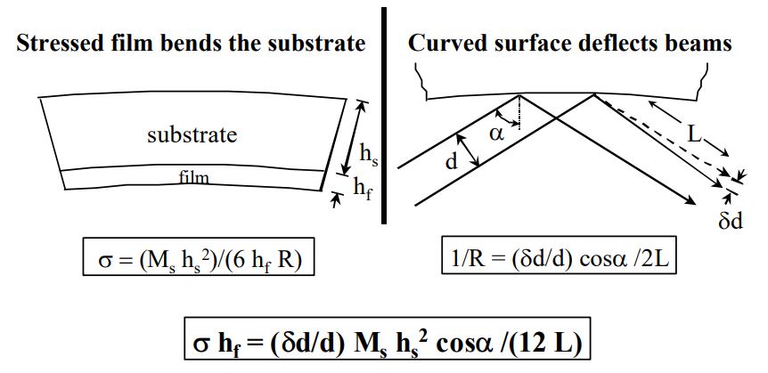
Figure 1. Film stress induces curvature in the film/substrate system. The curvature is detected by
measuring the deflection of parallel beams reflected from the film surface.
In the MOS technique (shown schematically in figure 2), multiple parallel beams illuminate the surface simultaneously and the beam positions are measured with a CCD detector. Because all the beams strike the surface simultaneously the technique is accurate even if the sample is vibrating (as is the case in many deposition systems). In addition, all the optics are fixed so that no motion of the sample or the optics is required.
The combination of parallel beam illumination and CCD detection result in a system that is capable of measuring a radius of curvature as large as 50 km on a benchtop apparatus; typical sensitivity for in-situ measurements is 4 km. This corresponds to a sensitivity in the product of film stress and film thickness, σhf , of 0.1 GPa-nm on Si wafers with 100 μm thickness. In other words, stress of 0.1 GPa can be measured on a film of 1 nm thickness, or 0.1 MPa on a film of thickness 1000 nm. This corresponds to the stress from 0.1 monolayer of Ge deposited epitaxially on Si.
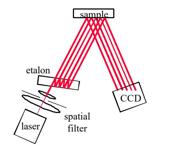 Figure 2. Schematic of MOS apparatus for measuring film stress. Multiple
parallel beams reflect simultaneously from the surface. The beam positions are
measured by the CCD camera.
MOS Technique for Thickness Monitoring
In addition to monitoring film stress, MOS measures film thickness in real-time for semitransparent films. The measurement is based on interference between the light beams reflected from the top surface of the film and from the film/substrate interface (see figure 3). If the film is not too absorbing, interference between the reflected beams results in a modulation of the reflected intensity. The reflected intensity is at a minimum when the beams interfere destructively, a condition that occurs when the layer thickness, d, satisfies the relation:
![\[ d = (2n+1) \frac{\lambda}{4 \sqrt{\varepsilon}\, cos \ \alpha} \quad \quad (3) \]](https://k-space.com/wp-content/ql-cache/quicklatex.com-fa212602fc0e3b9bc8862ae65040c092_l3.png "Rendered by QuickLaTeX.com")
where n is a positive integer, ε is the dielectric constant of the film, α is the angle of incidence and λ is the wavelength of the light. The period of the intensity oscillations is used to determine the growth rate of the film. In addition, the amplitude of the intensity oscillations depends on the reflectivity of the interfaces, so it is also a probe of surface morphology during growth.
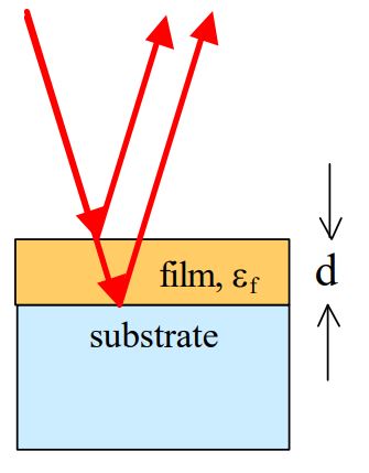 Figure 3.The measurement is based on interference between the light beams reflected from the top surface of the film and from the film/substrate interface.
Implementation of MOS on CVD Reactors
When utilizing MOS for stress monitoring in CVD, there are certain criteria that must be met. These are discussed below.
Optical access – MOS requires that the incident laser beams are able to illuminate the sample and that the reflected beams can be detected. Although many CVD systems use transparent reactor tubes, typically the glass is not of sufficient quality to allow passage of the beams without distortion. Optical access is usually better accomplished by access through viewports in the reactor, set up so that the angle of incidence equals the angle of reflection, i.e., conditions corresponding to specular reflection. For vertical reactor geometries, this can be accomplished by incorporating windows into the end caps. For horizontal geometries, this may require modification of the reactor tube. The illuminated region on the sample is typically on the order of 1 cm x 0.2 cm for stress measurement along one direction. Since the beams can be brought in nearly vertical to the sample, the incident and reflected beams can often be brought in through the same viewport.
Window heating – If the windows are too near the hot zone, active cooling may be necessary to achieve maximum sensitivity. Heating of the windows can lead to index of refraction changes that distort the apparent spacing of the beams. Active cooling can also reduce coating of the windows, which reduces the intensity of the beams. In many applications where maximum sensitivity is not required, absorption in the windows can be compensated for by increasing the laser power and the windows can be cleaned between growth runs.
Sample heating – Non-uniform sample heating can result in thermally-induced curvature that is unrelated to stress in the film. For instance, a temperature gradient from the front of the sample to the back will lead to thermal expansion differences that will curve the sample. Similarly, lateral temperature gradients will lead to non-uniform curvature in samples with films deposited on them. The significance of non-uniform sample heating can be determined by heating a wafer of substrate material with no film deposited and measuring the curvature change during heating cycles. The presence of gases may affect the thermal gradients in the sample, so introducing an ambient pressure of inert gas with cooling capabilities comparable to the processing gas is also a good idea. Although the bare wafer will not respond exactly the same as a wafer with a thin film, the measured curvature will give an indication whether thermally induced curvature is significant relative to the stresses being measured.
Even in heaters that achieve good steady-state uniformity, transients may occur when the temperature is changing that cause curvature in the sample unrelated to stress changes in the film. For this reason, care should be taken in making measurements of stress when the sample temperature is changed. Tests of similar heating conditions without deposition should be performed to rule out the effects of thermally-induced curvature during measurements of stress.
Sample rotation – Rotating disk reactors represent a particular problem since wobble of the sample leads to precession of the reflected beams as the sample rotates. This problem can be eliminated by synchronizing the acquisition of the MOS beam spacings with the sample rotation, so that the beams are always acquired at the same stage in the rotation. This is easily accomplished by using a gated video camera and taking advantage of the triggering capabilities of the MOS software. This approach has been used successfully on a rotating disk reactor where the sample rotation rate is 1200 rpm; motion of the beams on the CCD array was effectively eliminated using this technique.
Sample mounting – Because the MOS system determines stress from wafer curvature, the sample must be free to bend while the film is being deposited. For many reactor configurations, it is sufficient to allow the sample to be held in place by gravity. For reactors where the sample is mounted vertically, a sample mount with a retaining ring that does not exert any force against the substrate is required. The sample holder effectively forms a “cage” around the sample, keeping it in place but not exerting force on the wafer surface. Care must still be taken to make sure that the sample does not get constrained by the sample holder and is free to bend. For rotating disk reactors, a retaining ring can also be used to hold the sample captive without exerting any force on the surface. If this kind of sample mount is not possible, the sample may be held fixed at one end to form a cantilever. Curvature in this arrangement may lead to a large deflection of the beams and limit the degree of curvature that can be measured. In addition, the cantilever arrangement is very susceptible to induced vibrations so that the noise in the measurement may increase.
Sensitivity – As described in equation (1), the curvature is inversely proportional to the square of the substrate thickness. Using the thinnest possible substrates can greatly enhance the stress sensitivity by creating the largest change in curvature possible for the film stress. This must be balanced against the difficulty of handling extremely thin substrates and the added expense.
MOS Measurements of CVD Growth in GaN Films
To show the application of MOS in CVD growth, some results from the growth of GaN on sapphire substrates is shown here. Further details of these studies may be found in the publication cited below3 . The apparatus used for these measurements is shown schematically in figure 4. The films were grown in a rotating disk reactor where the sample rotation was 1200 rpm. The sample was heated inductively using RF Coils so that growth temperatures as high as 1350°C could be achieved. The MOS system was mounted vertically above the reactor. A small window in the endcap allowed optical access to the sample. The data acquisition was synchronized with the sample rotation to reduce the effect of wobble of the sample during measurement.
Real-time measurements of high temperature GaN growth are shown in figure 5. Initially, a low temperature buffer layer was grown at 550°C. The data in the figure corresponds to the subsequent growth of a high temperature GaN layer at 1050°C. The reflected intensity signal shows oscillations due to interference between the surface and the buried film/substrate interface; each period of oscillations correspond to approximately 124 nm of growth. Note that the amplitude of the oscillations changes during growth. The small amplitude of the initial oscillations is due to roughening during the early stage nucleation of the film (0 – 0.4 μm). After the film has attained a smooth growth morphology the amplitude of the oscillations is constant, indicating the presence of a smooth growing surface consistent with post growth characterization.
3 S.J. Hearne, E. Chason, J. Han, J.A. Floro, J. Fiegel, J. Hunter, I.S.T. Tsong, “GaN Stress Evolution during MetalOrganic Chemical Vapor Deposition”, Applied Physics Letters 74, 356 (1999)
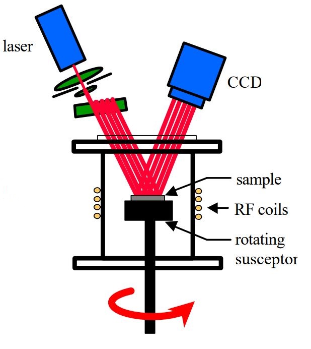 Figure 4. MOS system on rotating disk CVD reactor used for GaN growth.
The slope of the stress*thickness is constant in this region of growth, indicating that the stress in the film is constant. The stress in the film can be determined by dividing the measured stress*thickness by the film thickness to obtain a growth stress of 0.26 GPa. The sign of the curvature indicates that the stress is tensile. This result allows us to know the state of stress of the film during growth at temperature. It eliminates the need to extrapolate over a large temperature range from room temperature measurements, especially difficult when the thermal expansion coefficients are not well known.
In addition to measuring the actual stress during growth, MOS can determine the critical thickness at which stress starts to relax. For brittle, tensile films such as GaN, this corresponds to the onset of crack formation. MOS measurements of the onset of cracking are shown in figure 6. In this case, a high-temperature layer of GaN, 0.7 mm thick, is grown first. At the vertical line indicated in the figure, the growth of Al0.17Ga0.83N is initiated. The slope of the measured stress*thickness increases during the Al0.17Ga0.83N growth indicating that this layer has a tensile stress of 1.33 GPa, significantly higher than the stress in the GaN layer. After 0.63 mm of Al0.17Ga0.83N deposition, there is a sudden decrease in the measured stress*thickness, corresponding to the onset of crack formation. Determining when cracks begin to form by ex-situ characterization methods would require the growth of many samples. Using MOS, the critical thickness can be determined during a single growth run, making it possible to explore a much larger range of deposition parameters.
 Figure 5. MOS measurements of GaN growth at 1050°C. The stress-thickness (σhf) is proportional to the curvature.
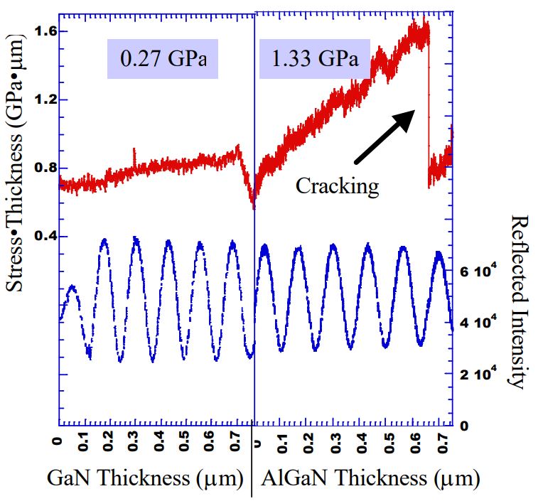 Figure 6. MOS measurements of GaN growth followed by Al0.17Ga0.83N. The sudden decrease in the stress-thickness
at 0.63 mm corresponds to the onset of crack formation.
