
Application Notes : kSA BandiT PV – Thin-Film PV Process Monitoring
Version: 1.0
- Introduction
- BandiT PV Technology
- Optical Band Gap
- Sample Temperature
- Parameter Monitoring
- System Integration
- Summary
Thin-Film PV Process Monitoring
THIN FILM PROCESS MONITORING FOR CIGS, CDTE, & CIS PV MATERIALS
REAL-TIME:
- Optical Band Gap
- Film Thickness
- Absorption Profile
- Surface Roughness
- Temperature
- Compatible with all deposition systems and substrate types
- Multiple probe technology for integration into production deposition systems
Introduction
Solar power is our largest energy resource and can provide a clean, sustainable source of energy. The use of solar power is expanding rapidly, but according to a recent Department of Energy report, “with present technologies, even assuming continued rapid growth, solar cells are predicted to only supply about 5% of the huge amount of carbon-free energy we will need by 2050”.
A key factor in producing the highest efficiency cells at the lowest cost will be the successful deployment of automated high volume production with tight process control. To achieve this goal, it is essential that monitoring methodologies be implemented that will lead to higher conversion efficiency and reduced manufacturing costs. This includes implementing in-line metrology tools which monitor the performance metrics of the thin-film photovoltaic materials being produced, so that the manufacturing process variables can be controlled and optimized in real time.
These approaches have been implemented with great success by k-Space in the semiconductor and optoelectronic device industry (improving the yield of microelectronic chips, high brightness LED’s, and diode lasers). However, this level of control over the manufacturing process has not yet been implemented for solar panel manufacturing.
k-Space manufactures state-of-the-art in-situ, real-time thin-film deposition monitoring tools, and has over 17 years of experience in the thin-film metrology field. The application of these proven kSA technologies to in-line PV manufacturing is a natural extension of it’s product line, as the most promising PV materials are based on thin-film semiconductor materials. The uniformity, thickness, band gap, and other physical properties are all critical parameters which influence PV device performance. In this technical note, we describe the use of our new k-Space BandiT PV system for monitoring today’s leading thin-film PV materials and how it can be used in the production of these materials.
kSA BandiT PV Technology
kSA BandiT PV technology is based on real-time spectroscopy of light diffusely reflected light from a semiconductor. A schematic of the functional components within the BandiT PV system is shown in Figure 1. A quartz halogen lamp supplies the light which is focused onto the sample. The diffusely reflected light is then collected at a non-specular angle using a lens system. The light is coupled to a high-speed, solid-state spectrometer. The spectrometer can be one of two basic types: visible, which uses a back-thinned Si camera, or near infrared (NIR), which is based on an InGaAs photodiode array. Light coupling is done using fiber optics. An integrated reflectance probe, which combines outer fibers for light output and a central fiber for signal detection, can also be used, resulting in a very small optical probe footprint, greatly simplifying integration into deposition tools. By virtue of the fact that reflected light forms the basis of the signal, there is no need to have access to the backside of the sample. This approach is therefore applicable to devices which are metal back coated, flexible, or otherwise opaque. All components used are solid state, with no moving parts, to ensure highest performance and reliability
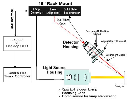 Figure 1: Main components used in the kSA BandiT PV process monitoring system.
Optical Band Gap
Typical diffuse reflectance spectra obtained with the kSA BandiT PV system for CIGS is shown in Figure 2. The signal to the left of the absorption edge (also called the “band edge” or the “optical band gap”) is light of sufficient energy to be above the band gap of the material, and therefore is absorbed. The signal to the right of the absorption edge has energy less than the band gap of the material and therefore is transmitted through the material. The transition from absorbing to transmitting defines the ‘band edge’ or optical band gap of the material. Knowledge of the wavelength of the absorption edge (Optical Band Gap) is critical to understanding the performance of PV materials. k-Space has been measuring this important semiconductor parameter for over 8 years. We have demonstrated the capability to measure this for the major PV materials being manufactured today, including cadmium sulfide (CdS), cadmium telluride (CdTe), and copper indium gallium diselenide (CIGS) — see Table 1. This can be done in real time during film deposition and/or post-processing. For example, postdeposition chemical and heat treatment is critical to the performance of CdTe-based modules.
| Material | Band Gap 300K (eV) | Corresponding BEW (nm) | Spectrometer Type |
|---|---|---|---|
| CdS | 2.4 | 500 | Visible |
| CdTe | 1.5 | 800 | Visible/NIR |
| CIGS | 1.0 | 1200 | NIR |
| Si | 1.1 | 1100 | NIR |
| GaAs | 1.4 | 900 | NIR |
Table 1: Typical band gap values and corresponding band edge wavelengths (BEW) Of PV semiconductor materials at 300K
 Figure 2: Typical kSA BandiT PV spectra for determination of optical band gap of CIGS
Sample Temperature
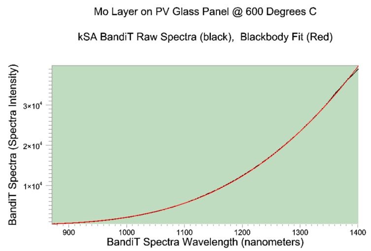
The measured optical band gap has a nearly linear dependence on temperature. This temperature dependence forms the basis of band-edge thermometry (BET), which has been utilized in the kSA BandiT semiconductor temperature measurement systems. kSA bandedge based technology relies upon the direct semiconductor optical absorption shift with temperature (band gap dependence on temperature). By fitting the optical absorption edge of the semiconductor in real time and using substrate-specific, kSA-generated calibration files, measurement accuracy and repeatability are guaranteed and unmatched by any other optical temperature monitoring technique. Insensitive to changing viewport transmission, stray light sources, and signal contribution from substrate heaters, kSA BandiT provides a valuable solution for temperature monitoring where pyrometers cannot measure. Compatible substrate materials and thin-films used in PV applications include InP, GaAs, GaP, Ge, CIGS, CdS, CIS, CdTe, Si, and most common semiconductor materials. All material temperatures can be measured from room temperature and higher using the band-edge technique. Please see the kSA BandiT product datasheet for additional information. kSA BandiT also combines a new, patent-pending Blackbody emission monitoring technology whereby the spectral radiation intensity of a sample is fit in real time to Planck’s equation to determine temperature. Direct chamber calibration via the band edge technique or high temperature blackbody auto-calibration ensures run-to-run repeatability and unmatched resolution (better than 0.1°C). kSA BandiT Blackbody technology is compatible with all semiconductor substrates as well as metal films from 300 ºC and higher. This technique is used for direct temperature measurement of the metal foil or film before the PV semiconductor layers have been deposited. Please see the kSA BandiT BlackBody technical note for additional information.
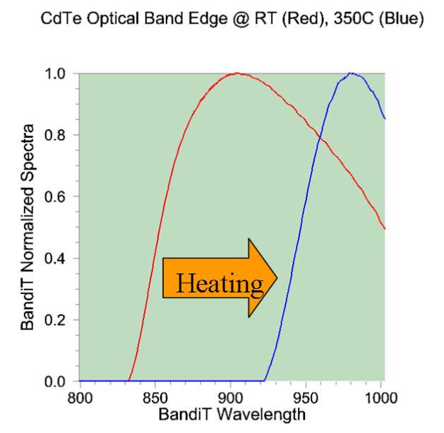
Figures 3 & 4: Typical kSA BandiT PV Band Edge and BlackBody Temperature Spectra
Parameter Monitoring
Film Thickness Monitoring
Another parameter critical to the performance of PV devices is the active layer thickness. An approach that lends itself to real time, in-situ measurements is based on analyzing the interference fringes observed in the reflectance spectrum from a film. Spectral reflectance spectra from thin films exhibit interference patterns due to light interference based on the film’s thickness (Figure 5). Provided that the film’s refractive index dispersion is known, the film thickness can be determined by analyzing the extrema positions of the interference fringes.
The fact that PV materials can be quite rough, and in fact are often intentionally roughened to increase solar absorption, can make thickness measurements more challenging. Nonetheless, by using a sensitive NIR spectrometer with a range that extends out to 2200 nm, signal levels are sufficient to enable precision at the one percent level or better.
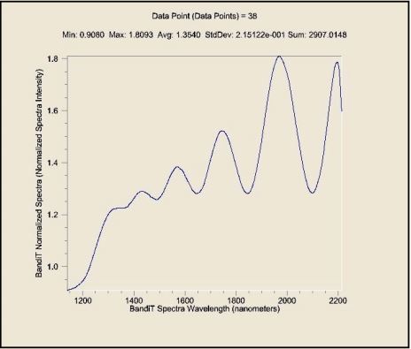 Figure 5: CIGS on glass interference fringes
Optical Absorption Profile
In addition to providing important optical band gap information in real-time, kSA BandiT PV can also analyze and compare the actual optical absorption shape profile of the material. With this method, the absorption spectra vs. wavelength can be monitored and tuned for abruptness of the interface at the optical band gap. In this fashion, the materials properties can be modified to provide the desired steep interface through process tuning or heat treating. An example of two different materials with different absorption profiles are shown in Figure 6.
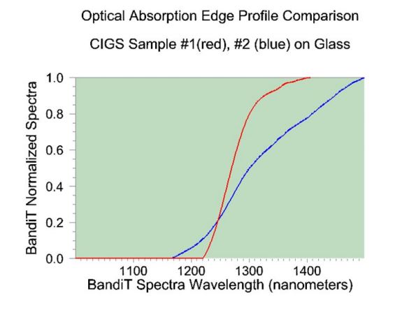 Figure 6: CIGS Absorption Shape Profiles
Surface Roughness
Surface roughness is one of the critical parameters affecting solar module efficiency. These surfaces are often intentionally roughened during the deposition process, as an optimally textured surface will absorb more solar radiation than a perfectly smooth one. However, carrying this too far can lead to a reduction in efficiency due to light scattering. Thus having access to in-situ roughness measurements in real-time can be important in order to strike the optimal balance. Roughness is typically measured using stylus-based profilometry or some other ex-situ method. However, this is not suitable for in-line measurements during manufacturing.
 Figure 7: “Above-Gap” portions of spectra showing difference in
kSA BandiT PV can get a relative measure of roughness by looking at the “above-gap” scatter from the surface. In theory, any light that has a wavelength sufficiently above the band gap energy should be completely absorbed by the semiconductor layer(s). However, as shown in Figure 7, we can observe signal changes in this region, due to scatter from the rough surface. The amount of scatter is a direct indication of the relative roughness of the surface. We therefore can sum the “above-gap” intensity to determine a relative roughness metric. This metric may also be calibrated directly against a sample of known surface roughness, providing a real-time, in-situ quantitative roughness parameter.
Production PV Deposition System Integration
kSA BandiT PV has been designed for installation onto commercial PV material deposition systems. By using multiple optical probes and optical multiplexing of the signals, a single kSA BandiT PV system can be used to obtain all important material characterization parameters in real-time during deposition on glass or metal foil samples. Because kSA BandiT PV does not require a specular geometry with respect to light source and detector, probe placement is simple and flexible, making BandiT PV easily adaptable to today’s vast array of PV substrates and manufacturing lines. A schematic representation of the integration hardware is shown in Figure 8. With up to 16 optical probes and coaxial fiber optic cable bundles delivering both light source and returning diffuse signal from the sample, kSA BandiT can measure and synchronize multiple measurement points across a panel in real-time. This probe placement flexibility identifies process variances of optical band gap, surface roughness, thickness, and temperature as a function of both process time (linear) and horizontal sample position.
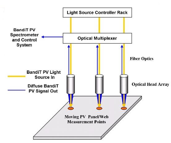 Figure 8: kSA BandiT multi-point measurement integration
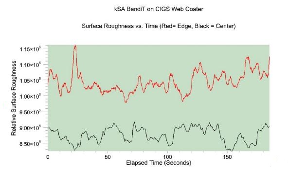
Figures 9 and 10 show data taken with a kSA BandiT PV system installed on a commercial web coating CIGS deposition system using metal foil substrates. Measurements were taken at two locations across the web to determine variations in both optical band gap and surface roughness. Important information related to variability and uniformity of the process was obtained for both lateral web position (i.e. center vs. edge of sample) and as a function of time. Correlations to surface roughness and optical band gap were also observed and will be described in future work. All data collected was available for immediate process control via TCP/IP interface, a standard feature of the kSA BandiT PV system.
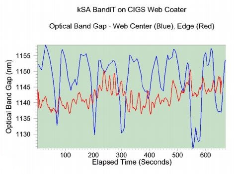
Figures 9 & 10 : Real-time optical band gap and roughness measurements at two points on CIGS coating system
kSA BandiT PV: Summary
The kSA BandiT PV system has been built using over 8 years of experience in in-situ semiconductor deposition monitoring. This technology has been directly applied to the real-time measurement of emerging thin-film photovoltaic materials such as CIGS, CdTe, CdS, and CIS. New, robust designs allow for the implementation of this technology into production PV manufacturing, yielding real-time determination of key process parameters such as optical band gap, surface roughness, thickness, and temperature. Please contact k-Space directly for more information or to request an on-site demonstration at your facility.
