
Application Notes : kSA MOS – Measurement of Stress Evolution
Version: 1.0
- Introduction
- Stress in Thin Films
- Measure thin film stress
- Multibeam approach (MOS)
- Interpreting measurements
- MOS Implementation
- Stress Evolution
- Coalescence
- Ag on SiO2
- High mobility material (Sn)
- Interrupt & Regrowth
- Stress measurements
- Sputter Deposition
- Whisker Growth
- Summary
- Acknowledgments
Measurement of stress evolution in thin films using
real-time in situ wafer curvature (k-Space MOS)
Eric Chason
Brown University, School of Engineering
- Intro to k-Space MOS (multi-beam optical sensor)
- theory
- capabilities
- analysis
- Examples
- polycrystalline films
- steady-state stress
- Scaling with D/RL
- stress vs thickness
- steady-state stress
- sputtering
- tin whisker formation
- battery materials
- polycrystalline films
Stress in thin films is a generic problem
Leads to decreased performance, deformation, failure
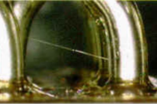
Cracks in Sn-Li electrodes
 Chao and Guduru. , MRS, 2012
Deformation in Ni MEMS devices
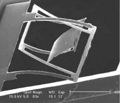 Matovic et al. , J. of Mech. Eng. Sci.2006
Stress voiding/electromigration
Stress in electroplated NiW
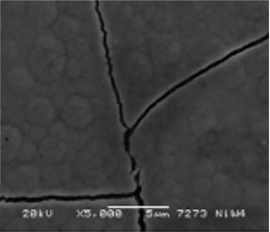 Mizushima et al. , Electrochimica Acta. 2006
Diamond on Si delamination
Want to:
understand stress,
control stress,
predict stress
→
First need to
measure it
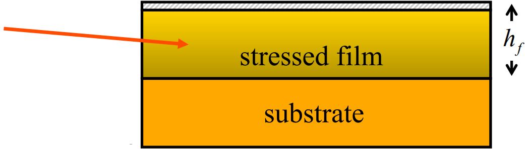
Measure thin film stress via wafer curvature
Stressed film bends the substrate
Stoney’s equation
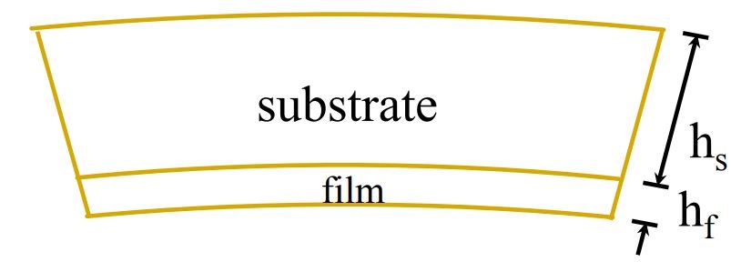
![\[ \kappa = \frac{1}{R} = \frac{6 \overline{\sigma}h_f}{M_sh_s^2} \]](https://k-space.com/wp-content/ql-cache/quicklatex.com-8a6b591d56715254781a480776693d0e_l3.png "Rendered by QuickLaTeX.com")
![\[ \mathit{For\, multiple\, layers:\quad} \frac{1}{R} = \frac{6}{M_sh_s^2} \sum_{i} \overline{\sigma}_i h_i \]](https://k-space.com/wp-content/ql-cache/quicklatex.com-40211708a7590cec50c5b04857a17997_l3.png "Rendered by QuickLaTeX.com")
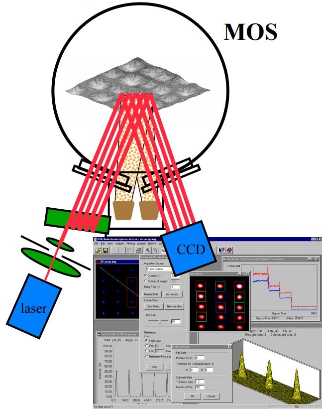
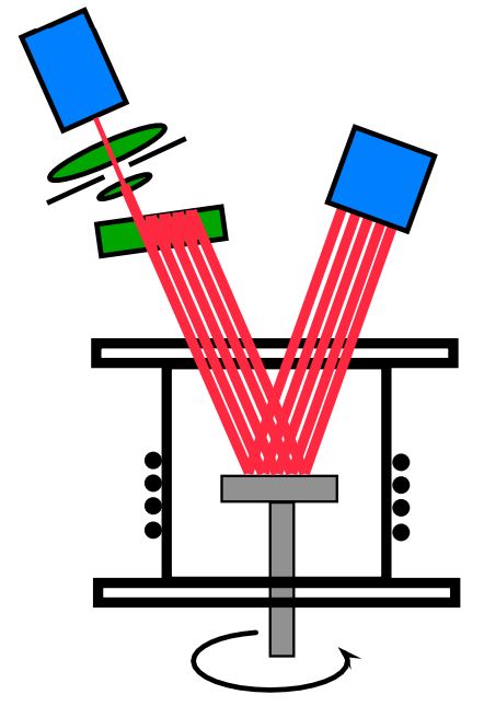
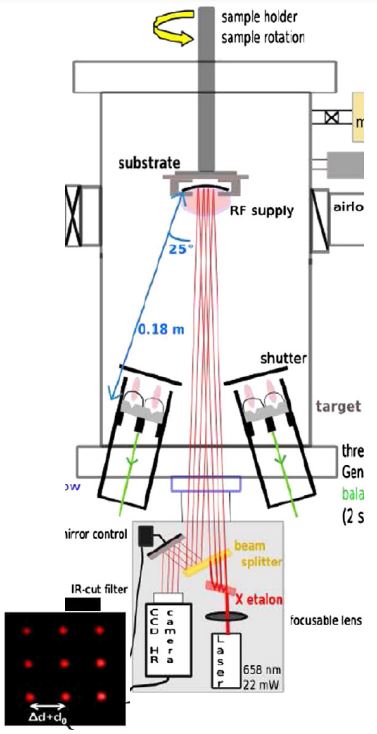
MOS (multi-beam optical sensor) Curved surface deflects array of parallel beams
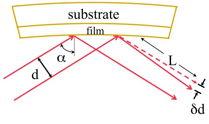
![\[ \frac{1}{R} = \frac{\delta d}{d} \frac{\cos \alpha}{2L} \]](https://k-space.com/wp-content/ql-cache/quicklatex.com-70ae55bf242fcd086e5c9cfcf2aa5804_l3.png "Rendered by QuickLaTeX.com")
Curvature measures product
of average stress x thickness
![\[ \overline{\sigma} h_f = \frac{\delta d}{d} \frac{M_sh_s^2 \cos \alpha}{12L} \]](https://k-space.com/wp-content/ql-cache/quicklatex.com-fb87d5738c183f879f0e02d24fbcb42c_l3.png "Rendered by QuickLaTeX.com")
Multibeam approach (MOS): easy to implement/robust
 Simple, stable optics (aligned outside processing chamber)
- in situ, real-time, high sensitivity
- R> 20 kM, σhf < 1 GPa-Å
- Can see 0.1 ML Ge on Si(001)
- System requirements:
- Ports to measure specular reflection
- Reflective surface (backside ok)
- Measurement technique
- Etalon produces array of parallel beams
- camera measures change in beam spacing (δd/d):
![\[ \Rightarrow \frac{1}{R} = \frac{\delta d}{d} \frac{\cos \alpha}{2L} \]](https://k-space.com/wp-content/ql-cache/quicklatex.com-9d0efd8a705b84090f17f21646ab5f67_l3.png "Rendered by QuickLaTeX.com")
Multi-beam technique reduces sensitivity to vibration
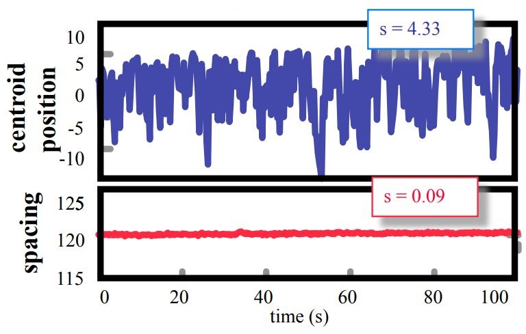 Measure difference between beams not absolute position
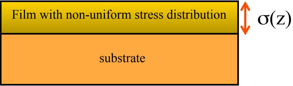
Interpreting curvature measurements
How does curvature relate to evolving stress distribution?
Average stress:
![\[ \overline{\sigma} = \frac{1}{h_f} \int\limits_0^{h_f} \sigma (z) dz \]](https://k-space.com/wp-content/ql-cache/quicklatex.com-bb35aedb78bd2f41d8826e37e6bba41d_l3.png "Rendered by QuickLaTeX.com")
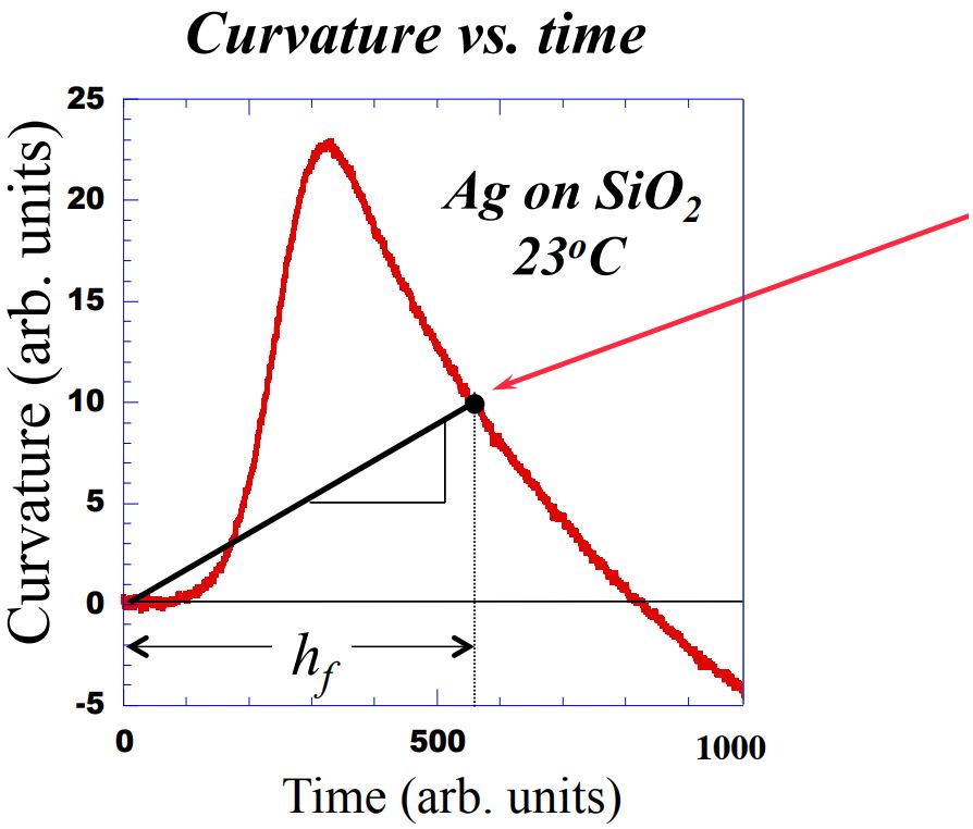
![\[ \overline{\sigma} = \frac{M_sh_s^2}{6} \frac{\kappa}{h_f} \]](https://k-space.com/wp-content/ql-cache/quicklatex.com-9cb6364e77a590eb8af90168621de064_l3.png "Rendered by QuickLaTeX.com")
- Thickness changes with time (deposition)
- Curvature changes as film grows over time
- Shows stress is not uniform throughout film
Stress distribution:
Study change of curvature with time
![\[ \frac{d \kappa}{dt} \propto \boxed{\sigma(h_f,t) \frac{\partial h}{\partial t}} + \int\limits_0^{h_f} \frac{\partial \sigma (z,t)}{\partial t} dz \]](https://k-space.com/wp-content/ql-cache/quicklatex.com-65ad18b6b47a2554a37dfcb373d9c210_l3.png "Rendered by QuickLaTeX.com")
(1) Stress in new layers
at the surface, σ(hf ,t)
![\[ \frac{d \kappa}{dh} = \frac{d \kappa / dt}{dh / dt} \propto \sigma(h_f , t) \]](https://k-space.com/wp-content/ql-cache/quicklatex.com-64ead065bf8a5395a1bd4fe79d1f6cc4_l3.png "Rendered by QuickLaTeX.com")
- Incremental stress proportional to slope of κ vs h
- But only if stress not changing in rest of film
Stress distribution:
Study change of curvature with time
![\[ \frac{d \kappa}{dt} \propto \sigma(h_f,t) \frac{\partial h}{\partial t} + \boxed{\int\limits_0^{h_f} \frac{\partial \sigma (z,t)}{\partial t} dz} \]](https://k-space.com/wp-content/ql-cache/quicklatex.com-7dbc74318b6f5693307d08a847d7b180_l3.png "Rendered by QuickLaTeX.com")
(2) Change in stress of
existing layers
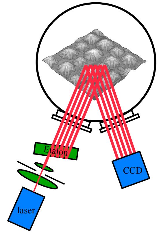
MOS Implementation
MOS can be implemented on many platforms
Deposition techniques:
- CVD
- sputtering
- PVD
- MBE
- PLD
- electrodeposition
MOS on GaN rotating
disk CVD reactor
(Hearne et al)
Materials systems:
- heteroepitaxy
- SiGe/Si, InGaAs/GaAs
- optoelectronics
- GaN, AlGaN, GaSb
- polycrystalline metals
- hard coatings
- DLC, a-C
- oxides
- TiO2 , CeO2
Examples from stress evolution studies
1. Residual stress in polycrystalline films
- Electrodeposition/evaporation
- Dependence on growth conditions, material
- Evolution with film thickness
2. Sputter deposition
- Effect of processing parameters (surface roughness)
3. Mechanical properties of Sn films
- stress leads to whiskers
- enhance stress relaxation
4. Strain in battery materials
- large volume changes
- associated with phase changes
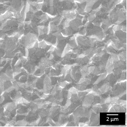
Features of stress evolution in polycrystalline films
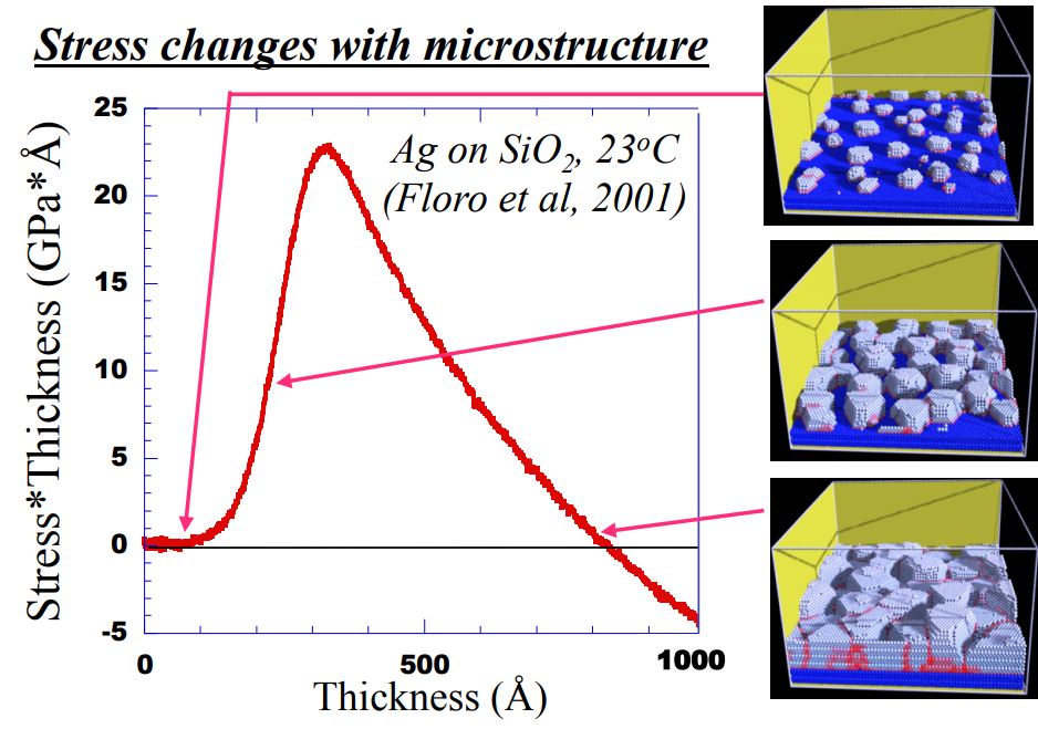
Stages of film/stress evolution:
- Nucleation
- Compressive or no stress
- Coalescence
- Tensile rise
- Continuous film
- Steady-state compressive (for high atomic mobility)
Stress depends on kinetics (temperature, material, deposition rate)
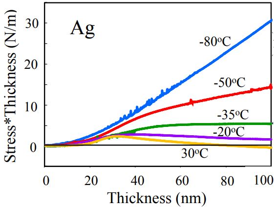
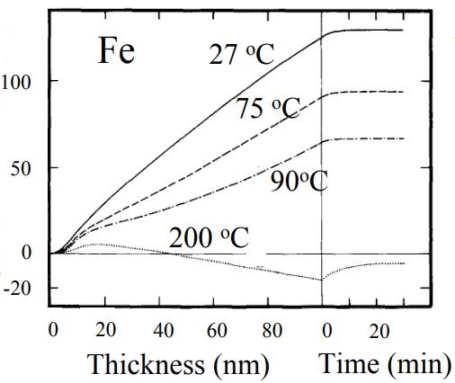
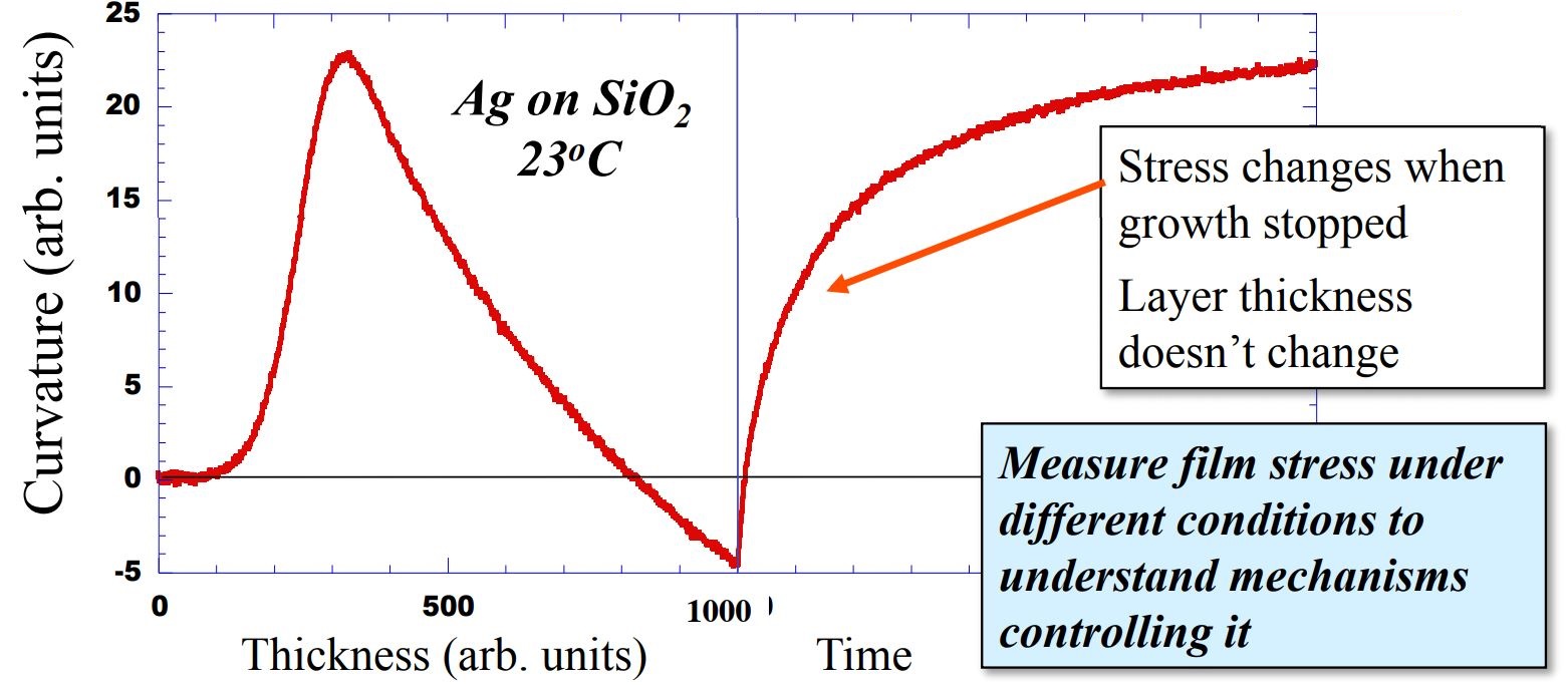
- Ag on SiO2
(Chason, Hearne, JAP 2013) - Fe on MgF2
(Thurner and Abermann, TSF, 1990) - Lower T, same growth rate:
- → more tensile
- At 30°C:
- Fe: tensile,
Ag: compressive
- Fe: tensile,
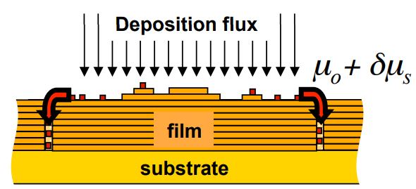
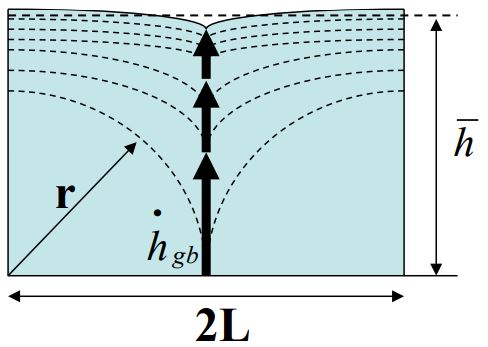
Consider stress as balance between different generation/relaxation mechanisms occurring at triple junction (top of grain boundary)
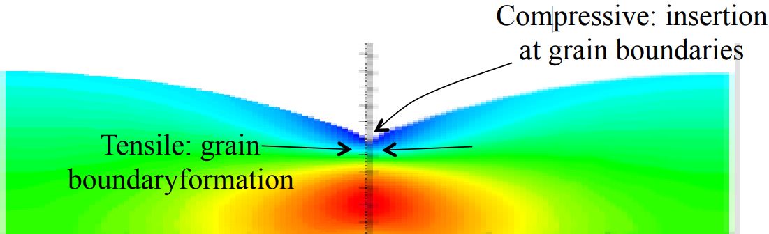
- Tensile → grain boundary formation
![\[ \sigma_T \propto \left( \frac{\gamma E}{L} \right)^{\frac{1}{2}} \]](https://k-space.com/wp-content/ql-cache/quicklatex.com-341af10adb2695234cbe7ef9bf2d0aa8_l3.png "Rendered by QuickLaTeX.com")
- Compressive → insert atoms into grain boundary (driven by surface supersaturation)
![\[ \sigma_C = \delta \mu_s/ \Omega \]](https://k-space.com/wp-content/ql-cache/quicklatex.com-1991726f1279b2ab11220cb732b29ebc_l3.png "Rendered by QuickLaTeX.com")
- Mediated by kinetic processes on surface:
- Growth rate R, diffusivity D, grain size L
Write equations for evolution of stress
Δµ drives atoms into or out of gb


2. 
Combine stress as grain boundary forms (tensile) with stress as atoms are inserted into it (compressive)
3. Induced Stress: 
Master equation for stress evolution at triple junction:
![\[ \frac{\partial \sigma_{tj}}{\partial t} = - \frac{4C_s M_f}{akT} \frac{D}{L} \cdot (\sigma_{tj} \Omega + \delta \mu_S \]](https://k-space.com/wp-content/ql-cache/quicklatex.com-e7c89fb781d59aa02f78aceb95e92f40_l3.png "Rendered by QuickLaTeX.com")
![\[ \sigma_{tj} = \sigma_C + (\sigma_T - \sigma_C) \cdot e^{- \Delta t_{tj} / \tau} \mathit{where}\ \Delta t_{tj} = a / \dot{h}_{gb} \]](https://k-space.com/wp-content/ql-cache/quicklatex.com-1a373e63a5437f17a01760296cebd6ca_l3.png "Rendered by QuickLaTeX.com")
hgb = Rate of growth of grain boundary
Steady state stress: dependence on growth rate
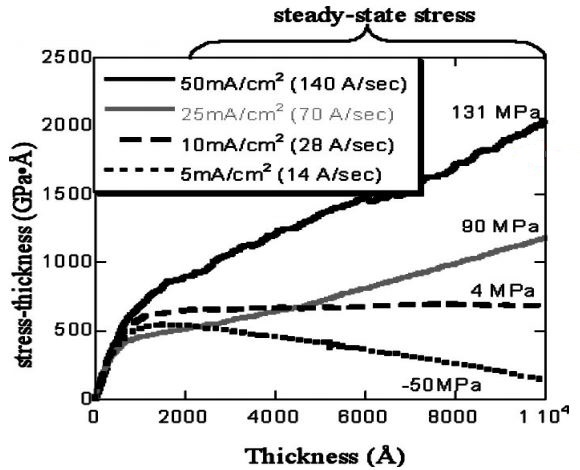
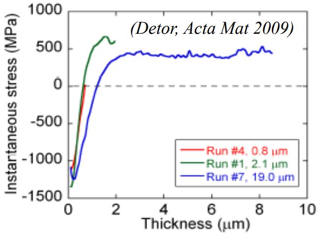
Electrodeposited Ni on Au, Hearne et al, JAP 97 (2005)
- Stress reaches steady-state (constant slope)
- Different σSS for each growth rate
- Model prediction:
![\[ \sigma_{SS} = \sigma_C + (\sigma_T - \sigma_C) \cdot e^{- \alpha D / RL} \]](https://k-space.com/wp-content/ql-cache/quicklatex.com-1718a2bec3a732bb247711495c6329d2_l3.png "Rendered by QuickLaTeX.com")
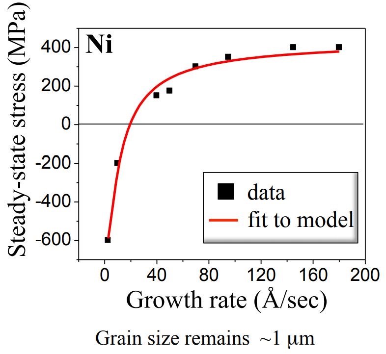

![\[ \frac{D}{RL} << 1 \quad \mathit{Low \ D, \ high \ R \rightarrow \ tensile} \]](https://k-space.com/wp-content/ql-cache/quicklatex.com-bd3fd85bcaac4670c638282fe56d751f_l3.png "Rendered by QuickLaTeX.com")
![\[ \frac{D}{RL} >> 1 \quad \mathit{High \ D, \ low \ R \rightarrow \ compressive} \]](https://k-space.com/wp-content/ql-cache/quicklatex.com-7db72e53c31dc39fd40f610b75a0d0d1_l3.png "Rendered by QuickLaTeX.com")
→Determines growth rate for
stress-free films
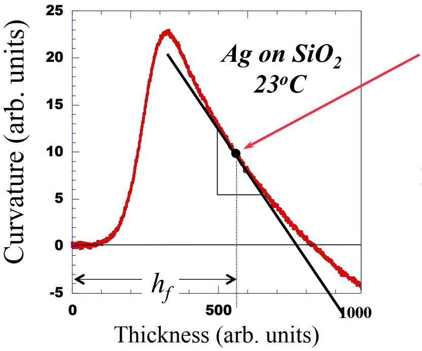
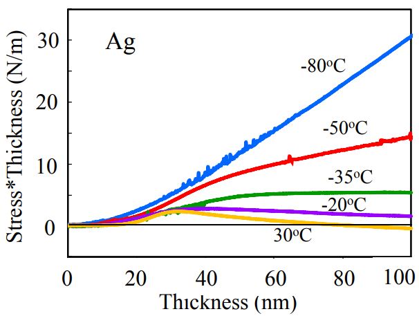
Stress vs thickness: effect of coalescence of islands
Data: Stress changes with thickness
- Depends on temperature
PVD Ag on SiO2 , (Hearne)

Model:
![\[ \sigma_i = \sigma_C + (\sigma_T - \sigma_C) \cdot \exp (- \frac{\alpha D}{L \frac{\partial h_{gb}}{\partial t}}) \]](https://k-space.com/wp-content/ql-cache/quicklatex.com-95c517842cf7ac1d71d9652b45334545_l3.png "Rendered by QuickLaTeX.com")
–  changes during coalescence
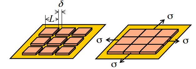
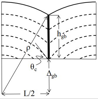
– Model islands as cylindrical caps to calculate grain boundary velocity
Grain boundary growth rate changes as film grows
Stress changes with grain boundary velocity
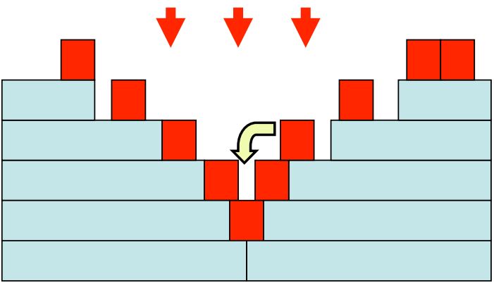
Consider process of coalescence
- Calculate how
 changes during coalescence
 - Model islands as cylindrical caps
- Initial spacing is L
Grain boundary velocity changes as islands grow
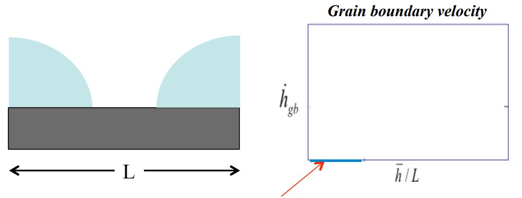
Before coalescence, 
(no grain boundary)
 Grain boundary forms at onset of coalescence
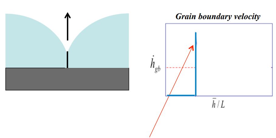 Grain boundary grows rapidly at first
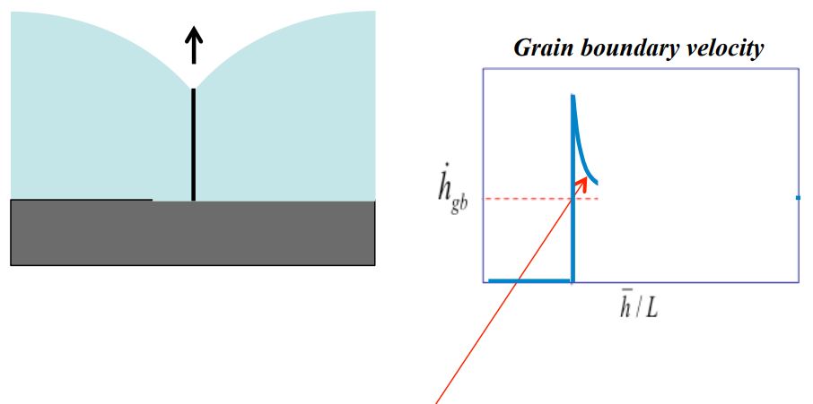 Slows down as film gets thicker
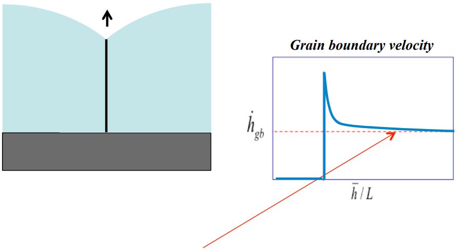
 approaches average growth rate (R) as film gets thicker (steady-state)
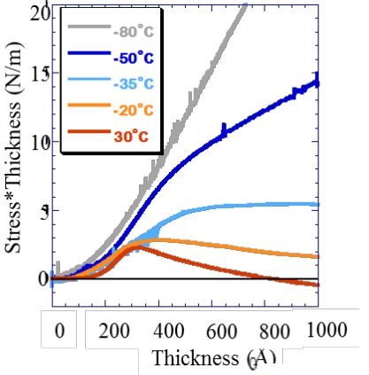
Model fits Ag on SiO2 data
Change atomic mobility (D) at constant R, L
PVD Ag on SiO2 , (Hearne)
Model: 
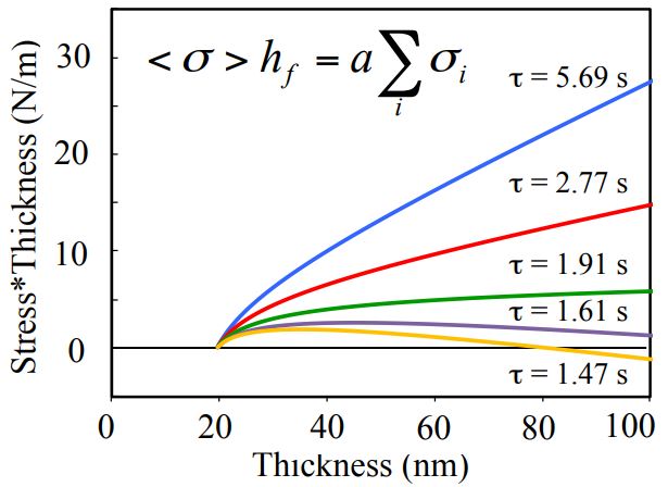
- Islands are cylindrical caps, contact angle ~68 deg,
- Fitting parameters: σc, σT , τ
- Use same σT (442 MPa) and σc (-359 MPa) for all temperatures
- τ different for each T (proportional to 1/D)
Role of grain boundary in high mobility material (Sn)
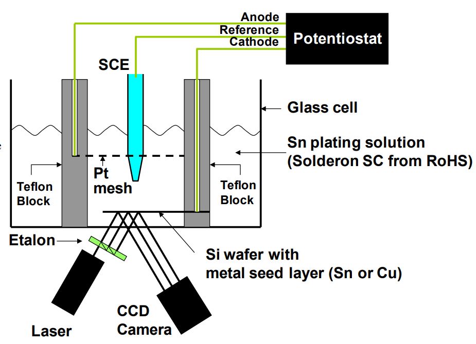
Monitor stress during electrochemical deposition

- Evaporate seed layer of Sn (1 µm)
- Electrodeposit Sn film at constant voltage
Stress behavior during interrupt & regrowth
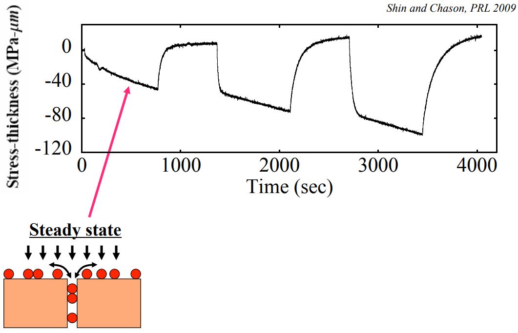
![\[ \sigma_{SS} = \frac{\sigma_T + (\alpha D / RL) \sigma_C}{1 + (\alpha D / RL)} \]](https://k-space.com/wp-content/ql-cache/quicklatex.com-de8543316ecfde937a722469dd42a993_l3.png "Rendered by QuickLaTeX.com")
Interpretation of stress behavior at interrupt & regrowth
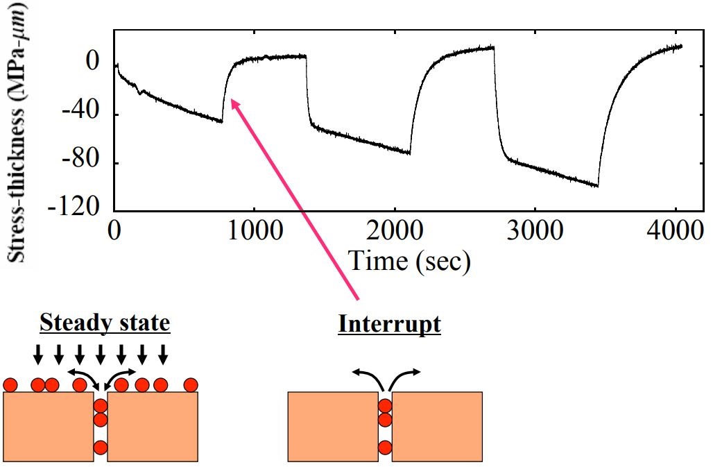
![\[ \delta \mu_S = 0 \quad R = 0 \]](https://k-space.com/wp-content/ql-cache/quicklatex.com-4e19aea5fed6916848872c816c8a112f_l3.png "Rendered by QuickLaTeX.com")
![\[ \sigma = \sigma_f + (\sigma_i - \sigma_f)e^{-t/\tau_{\mathit{relax}}} \]](https://k-space.com/wp-content/ql-cache/quicklatex.com-2bf7060973d946daae6602d2ae23ad37_l3.png "Rendered by QuickLaTeX.com")
Decay rate depends on layer thickness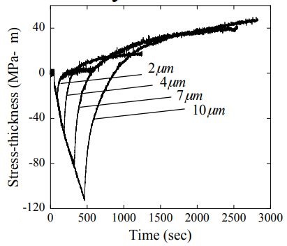
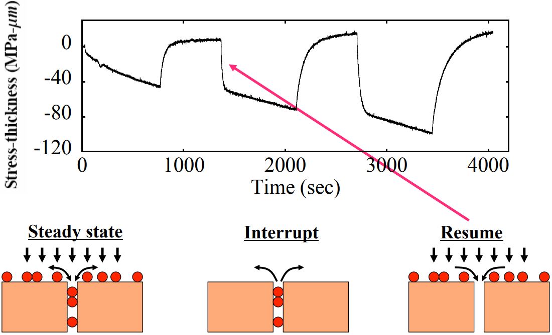
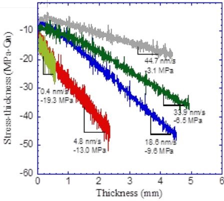
Stress measurements in electrodeposited Sn
Stress-thickness vs thickness – same slope after interrupts

Stress is independent of layer thickness:
- confirms role of grain boundary in stress evolution
Stress during etching
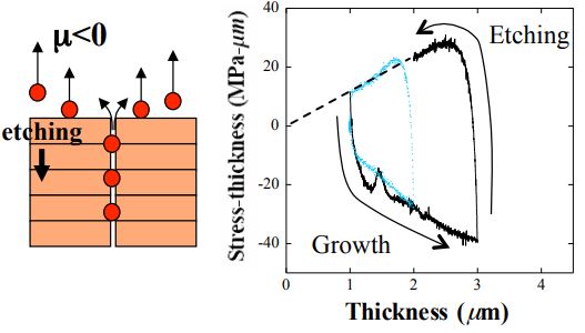
Equivalence between growth and etching:
- negative chemical potential on surface induces tensile stress in film
- confirms role of surface chemical potential in stress evolution
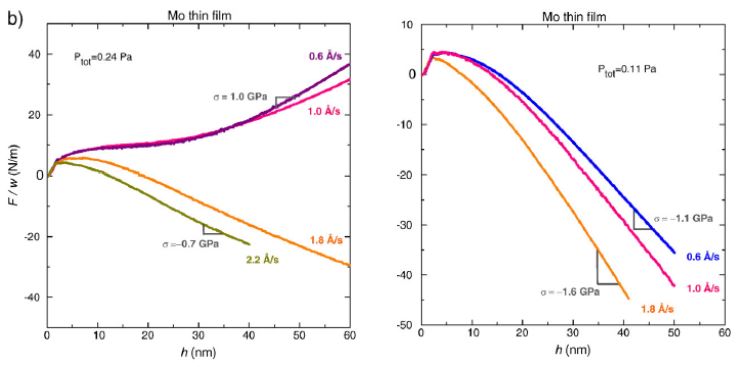
Stress evolution during sputter deposition
Additional parameters: ion energy, gas pressure
MOS with magnetron sputtering sources
(Mo films, Fillon, Abadias, et al. TSF 2010)
Lower pressure → more energetic particles
Stress becomes more compressive
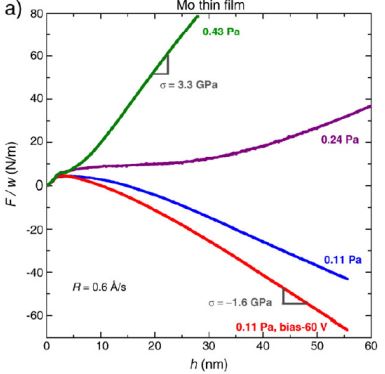
Dependence on growth rate different than evaporation
Don’t know grain size or grain evolution
Stress evolution during sputter deposition (LLNL)
Be targets for NIF: need films with low stress (thick > 100 µm)
Higher growth rate (power) → more tensile
Higher T → more compressive
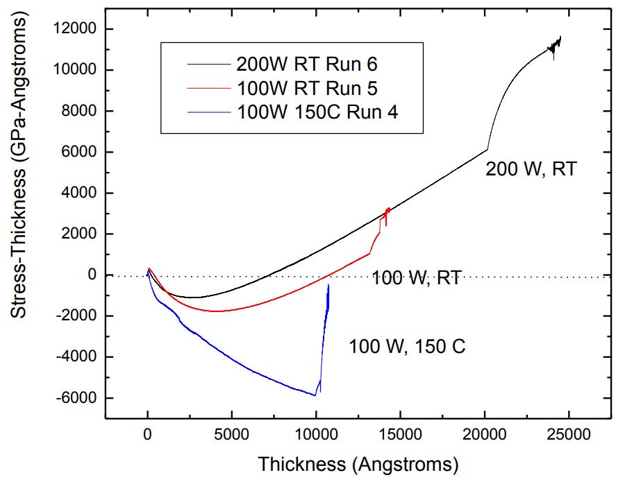
Be sputtering results (LLNL): effect of pressure
Lower pressure → more compressive initially
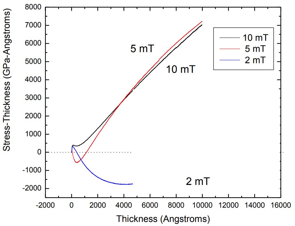
Why? Lower pressure means less scattering, more energetic incident particles: implant into surface, produce higher density
Be sputtering results
Lower pressure → more compressive initially
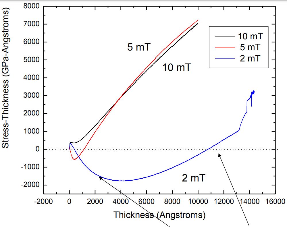 BUT: Incremental stress changes from compressive to tensile
as layer gets thicker → kept same temperature, growth rate
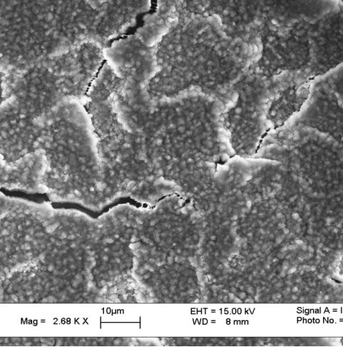
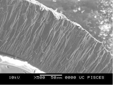
Reason: Stress change correlated with rougher surface morphology
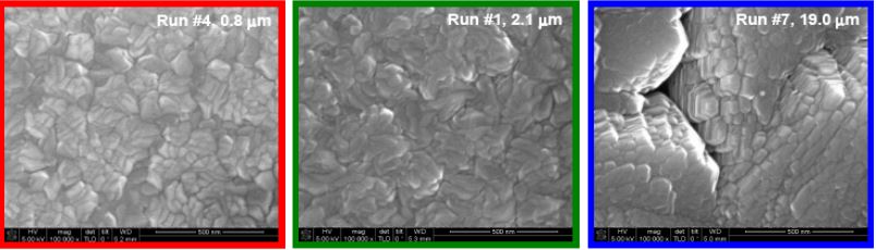
Film structure:
roughening instability
(Zepeda-Ruiz, APL 2010)
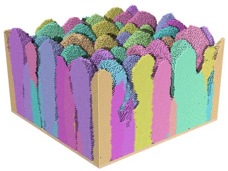
Porosity
vs depth

Greater roughness → Turns off compressive stress generation
Film becomes tensile
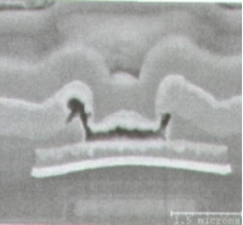
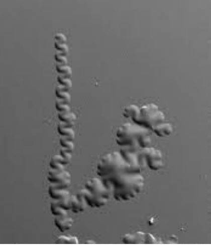
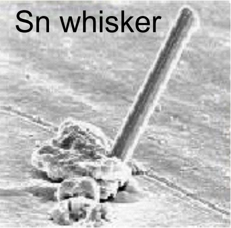
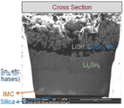
Sn whisker growth: driven by stress from IMC (intermetallic) formation
Whiskers form in Pb-free Sn coatings on Cu – cause systems failure (satellites, pacemakers)
IMC forms at Cu-Sn interface
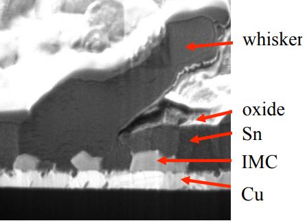
Measure stress evolution with MOS
Wafer curvature measures total force exerted by film.
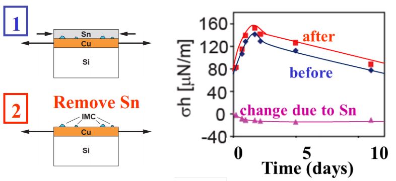
Remove Sn layer – change in curvature gives stress in Sn
Correlate IMC/stress/whiskering
(Chason & Jadhav, APL 2009)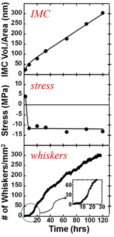
Reduce whiskering by enhancing stress relaxation
- Measure mechanical properties of layers:
- Sn and Sn alloys
- Find coatings that have low stress even after IMC grows
Use thermal expansion mismatch to create strain


Measure stress vs. strain for different films
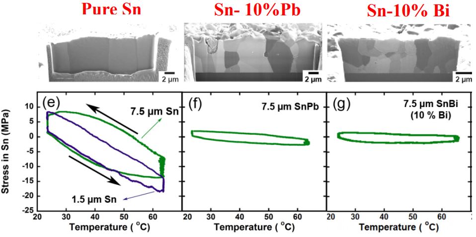
- These results agree with conclusions from whisker studies
- More relaxation with
- larger grain size
- thickness
- horizontal grain boundaries
Stress evolution during charging/discharging of batteries
(lithiation of Sn anode)
Put MOS on electrochemical cell
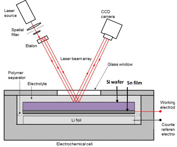
Simultaneously measure C-V and stress-thickness
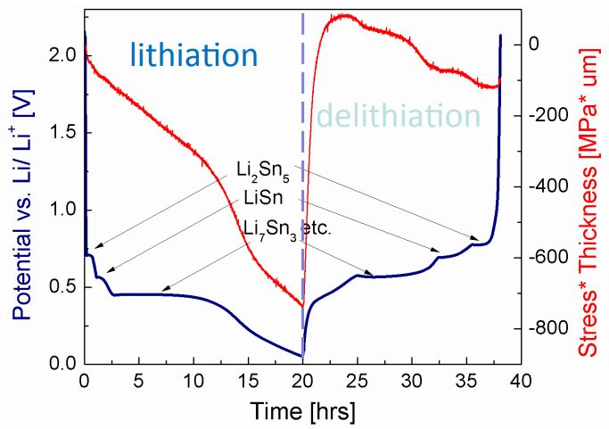
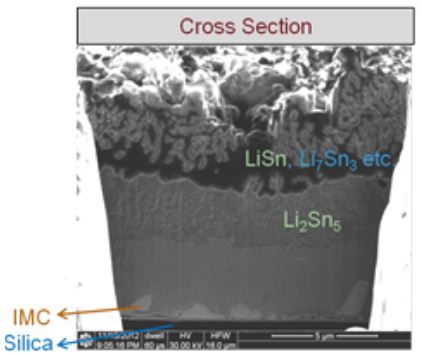
Measure stress associated with phase changes
Need to know layer thicknesses to interpret MOS data
(Chen, Guduru 2013)
Summary
- Multi-beam wafer curvature (MOS) enables stress evolution to be monitored in real-time
- useable on wide variety of platforms
- sensitive, robust, easy to interpret
- Stress dynamics provide more information than single stress measurement
- Key for
- modeling
- understanding sources of stress
- controlling stress (optimizing processing conditions
- Key for
- Frontiers
- Understanding multi-component materials
- Energetic particle effects
Take home point:
In situ monitoring useful for understanding stress evolution
Acknowledgments
Brown:
Jae Wook Shin (LAM)
Chun-Hao (Charly) Chen
Alison Engwal
Julie Zaskorski (REU)
Brittni Thomas (REU)
Nitin Jadhav
Tanmay Bandakhar
Allan Bower
Ben Freund
Brian Sheldon
Huajian Gao
Pradeep Guduru
K.S. Kim
Sandia:
Jerry Floro (UVa)
Sean Hearne (Sandia)
LLNL:
George Gilmer
Luis Zepeda-Ruiz
Alex Hamza
Chris Walton
Morris Wang
NIST:
Gery Stafford
k-Space:
Darryl Barlett
Chuck Taylor
Eric Friedmann
Roy Clarke
