
Application Notes : kSA MOS UltraScan – Patterned Silicon Wafers
kSA MOS UltraScan Performance Test Data: 200 mm Patterned Silicon Wafers
Version: 1.0
Introduction
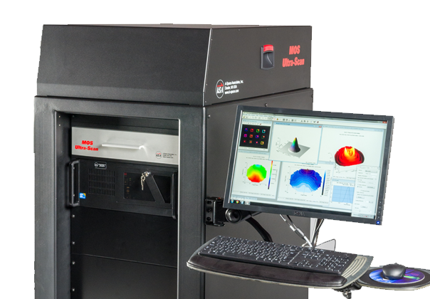
The kSA MOS UltraScan is a flexible, high resolution scanning curvature and tilt-measurement system. Based on the proven technology of our standard in-situ kSA MOS system, the kSA MOS UltraScan uses a laser array to map the two-dimensional curvature and stress of semiconductor wafers, optical mirrors, lenses— practically any polished surface. The standard system provides a 300 mm x,y scanning range with 1 μm scanning resolution. Scans are fully programmable for selected area, line scan, or full area map. The system also provides quantitative film stress analysis with full area map by first scanning the bare substrate and then rescanning the sample post-process.
Patterned Wafer Measurements
In order to demonstrate the effectiveness of the kSA MOS UltraScan instrument for curvature measurements
on patterned wafers, three types of scans were performed:
1. Simple line scan across the diameter of the 200 mm wafer over a range +60 mm to 60mm.
2. Low-resolution area scan of a 5mm radius circular area close to the center of the wafer.
3. Higher resolution area scan of a 2mm radius circular area close the center of the wafer.
4. Area Scan using a 2-D laser beam array (3 rows of 4 spots).

All three scans were made by reflecting a single linear array (Fig. 2) from the surface of the wafer and detecting the spot spacing D(t) on a CCD camera.
Note that curvature measurements in the kSA MOS UltraScan are normally made with a two dimensional array, but in this case, as a quick preliminary test, a one-dimensional array was used. In the measurements described here only the X-direction (in the plane of the wafer perpendicular to the wafer flat) is measured to provide an example of the expected performance. The measurements using a 2-D array can be expected to be even more precise and higher resolution, as well as providing curvature data in both directions (X and Y).
Scan 1: Measurement of Coarse Wafer Bowing
Fig. 3. shows a plot of the bow height of the patterned wafer in microns measured with a 10mm step size, along a line perpendicular to the wafer flat. The overall surface of the wafer is concave with the center (at approx. zero on the plot) displaced downwards by approx. 7 microns relative to the wafer circumference. The deformation is approximately parabolic. This would correspond to an overall compressive stress in the wafer coating.

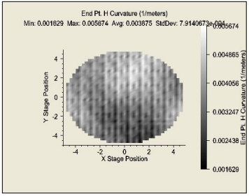
Scan 2: Low Resolution Area Map of Wafer Curvature
Fig. 4 shows a circular area scan of a 10 mm diameter portion of the patterned wafer close to its center. What is measured in the plot is the component of the curvature of the wafer in the X direction, in units of m-1. Note that 0.001 m-1 corresponds to a radius of curvature of 1 km (in other words the wafer surface conforms to a circle of radius 1km). One can clearly see the small variations in local curvature induced by the patterned metal electrodes. The curvature is quantified as a gray scale from 0.001 m-1 to 0.005 m-1. Note that the residual stress can be calculated from the curvature data in Fig. 4, (from Stoney’s equation) using the bulk wafer modulus. However it is clear that the relative variation is easily measured between the metal pads (low stress) to the region between the pads (high stress). Apparently the dark regions (low stress) in Fig. 4 correspond to the position of the metallizations. A word of caution here: the values of the curvature shown in Fig. 4 were not calibrated against an optical flat in these preliminary measurements. The software of the instrument will perform this calibration and automatically return accurate absolute values in a more careful measurement. These data only provided as an example to show that the instrument is capable of making the required measurements.
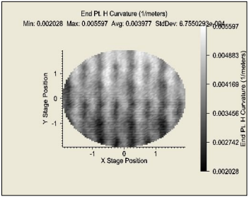
Scan 3: Area Scan with 50 Micron Step Size
Fig. 5 shows a higher resolution curvature scan with 50 micron step size. The overall variation in stress is similar to that shown in Fig. 3. Additional detail is seen in the image showing that the stress is not uniform along the lines between the pattern. The resolution (~50 microns) could be improved even more with the 2-D array (standard for kSA MOS UltraScan, but not used for this measurement because we wanted to get some preliminary results to you quickly).
Scan 4: Area Map of Patterned Wafer with 50 Micron Resolution
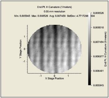
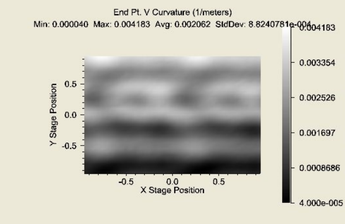
For comparison we ran two additional scans using he full 2-dimensional laser beam array. Fig. 6 shows the map of X component of the curvature, measured with 50 micron step size, and Fig, 7 shows the corresponding Y component (parallel to the wafer flat).
As expected the local curvature features measured with the 2-D array are very similar to those measured with a linear array (compare Fig. 5), except the spatial resolution is noticeably better. Also note that the curvature values are different in Figs. 5 and 6. That is because we did not calibrate either scan with respect to a standard optical flat. The relative variation shown in Fig. 6 is probably more accurate, but a proper reference scan would have to be taken to obtain absolute values. This was not done for this particular test. Fig. 7 shows the map for the corresponding Y-component of curvature the patterned wafer. Interestingly the curvature appears to be quite anisotropic, perhaps due to anisotropy in the patterning of the wafer. Also interesting is that the curvature changes sign, meaning that along the Y-direction (parallel to the wafer flat) the shape of the surface alternates locally from convex to concave (like the surface of a golf ball).
Asymmetry of MOS Data
Figs. 6 and 7 indicate quite clearly that the X and Y directions on the wafer are not equivalent and this asymmetry may be related to the asymmetry of the wafer pattern itself. A schematic of the pattern as seen in an optical microscope appears as follows:
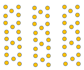
Clearly the contact pads are arranged in an asymmetric fashion. The horizontal (H) direction is different than the vertical (V) direction. In particular there is a larger spacing between the rows of metal pads along H than along V. This gives the impression of “stripes” on the wafer, both in the surface topography (Fig. 8) and in the kSA MOS UltraScan scans (Fig. 9).
In order to verify that the measurement of the curvature map is valid, and that the measurements do indeed correlate with the anisotropic geometry of the wafer pattern (Fig. 8) we performed several additional scans as follows. One of these tests is to measure a curvature map in one wafer orientation and then do the same measurement again with the wafer rotated through 90 degrees. Since both components of the wafer curvature are measured simultaneously with MOS, it is possible to test for anisotropy and also to test whether it is valid by checking if the observed curvature pattern rotates in the expected way as the sample is rotated. Such a test was performed as shown in Fig. 9. A significant anisotropy is observed which correlates well with the asymmetric geometry of the metallization pattern.
a)
b)

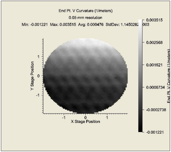
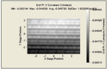
Fig. 9: 6mm x 6mm scan with 0.05 mm resolution. (a) wafer oriented with scan direction parallel to the H direction in Fig. 8: and b) after rotation of the wafer through approximately 90 degrees. Note that the vertical component of the curvature is measured in (a) whereas the horizontal component of the curvature is measured in (b) so that the wafer curvature is measured along the same axis on the wafer in both cases. The stripe-like features therefore rotate with the wafer, confirming that they are related to the actual wafer pattern and not some artifact of the MOS scanning method.
Note that while the two curvature maps shown in Fig. 9 should be identical except for a ~ 90 degree rotation, there are some noticeable differences. One is that the scale of the curvature shown on each plot is different and that is because we did not use a standard reference to provide an absolute calibration. Second, the small modulations of curvature along the “stripes” (Fig. 9a) are better resolved when the scan step is parallel to the stripes rather than perpendicular (Fig. 9b). Nevertheless, the overall appearance of the curvature map is very similar in both cases, as expected.
A magnified portion of the type of scan shown in Fig. 9(a) is shown in Fig. 10. The local distortions of the wafer surface can be seen quite clearly and, interestingly, the features in this curvature map (Fig. 10) correlate quite well with the actual metallization pad pattern (Fig. 8).
kSA MOS UltraScan demonstrated excellent sensitivity and high resolution sufficient to quantify the local changes in curvature induced by metallization patterning on a 200 mm silicon wafer. The anisotropy in the metallization pattern is clearly seen in the curvature maps, down to the level of the region around individual contact pads. Differences in curvature at a level of sensitivity of better than 0.001 m-1 are easily imaged by the kSA MOS UltraScan™ mapping technique.
