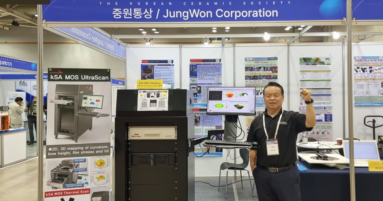
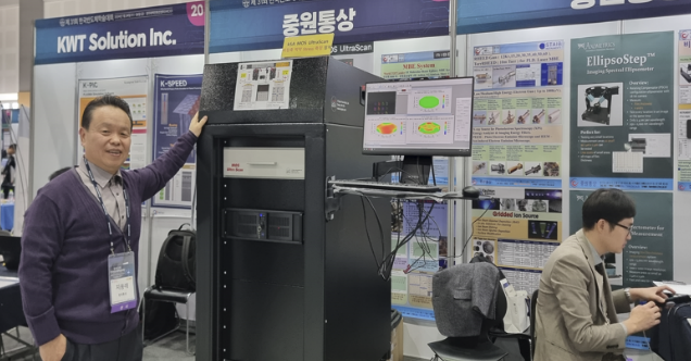
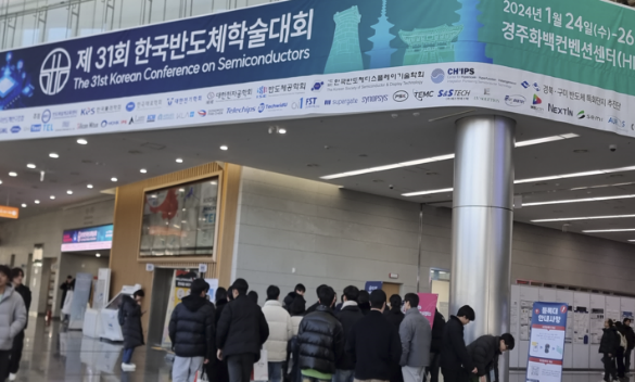
k-Space thin-film metrology solutions are proving to be a big hit at the many semiconductor and materials science shows in Korea. Our kSA MOS UltraScan made appearances at this year’s SEMICON Korea and at the Korean Conference on Semiconductors. The kSA MOS UltraScan then made its way to last week’s Korean Ceramic Society exhibition after being transported via “vibration-free vehicle.”
Great job by Jung Won Corporation, our sales representative for Korea. At each stop, the many scientists, researchers, and executives in attendance were provided a hands-on demonstration of the patented kSA MOS UltraScan.
These events reflect the growth and innovation of the semiconductor ecosystem in Korea, as well as the need for metrology tools to improve processes, extend innovation, and increase profitability.
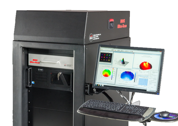
The kSA MOS UltraScan uses a laser array to map the two-dimensional curvature, bow, and stress of semiconductor wafers.
Click here to find out more about the kSA MOS UltraScan and our patented kSA MOS (Multi-bean Optical Sensor) technology.