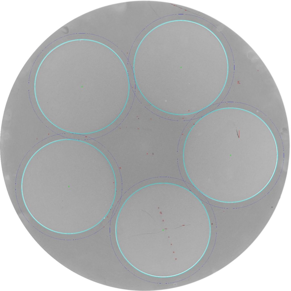
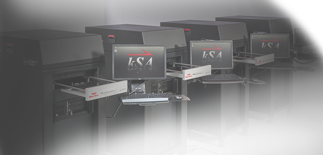
k-Space Associates, Inc. has added an exciting new feature to the kSA Emissometer that will make it an even more effective tool for detecting defects in MOCVD wafer carriers.
The kSA Emissometer is a state-of-the-art metrology tool designed to easily generate high-resolution diffuse and specular reflectance and total emissivity maps of MOCVD carriers. Variation in carrier emissivity correlates to temperature non-uniformity, which can lead to reduced device yield and growth run issues. This new feature makes the kSA Emissometer even more essential for fabs to help with early defect detection, and for carrier manufacturers to detect quality issues before they ship the carrier to their end user.
At the end of a carrier scan, this new feature displays the number of defects it detected and summarizes the number of the pocket defects, web defects, and halo-region defects. The software outlines the defect regions in the carrier image to easily identify their positions. The user can save the image files to examine or analyze later. This allows fabs to pull the defective wafer carriers before they cause an issue, and they can perform in-depth analysis later.
Senior Product Engineer, Greg DeMaggio stated, “We try to improve our products based on customer requests. This additional defect analysis was something our customer desired and we were able to implement it. The new capability makes their defect identification process easier, will ultimately lead to improved quality, reduced production costs, and is a great addition to the analysis capabilities of the kSA Emissometer.”
To learn more about the kSA Emissometer, visit our website at https://k-space.com/product/ksa-emissometer/.


